
Method of joining components

a technology of components and components, applied in the field of joining components, can solve the problems of difficult manufacturing of detectors with optimal performance, limited selection of materials and methods that are usable for the manufacturing of detectors, and damage to electronic components

Inactive Publication Date: 2006-06-27
FAUN DATA
View PDF3 Cites 1 Cited by
  • Summary
  • Abstract
  • Description
  • Claims
  • Application Information

AI Technical Summary

Benefits of technology

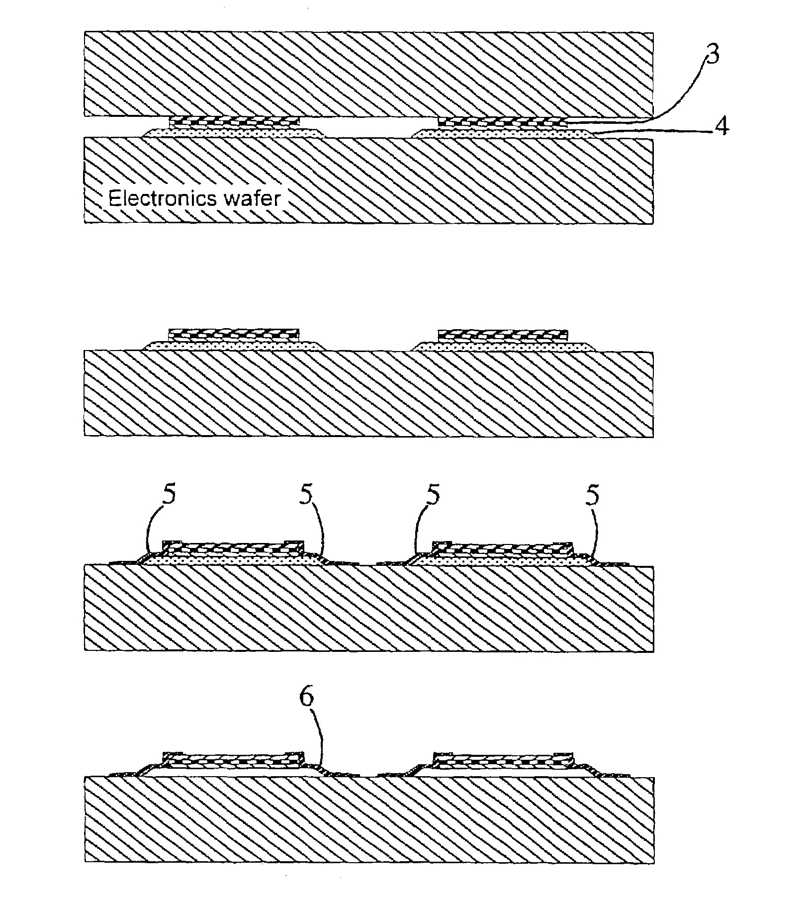
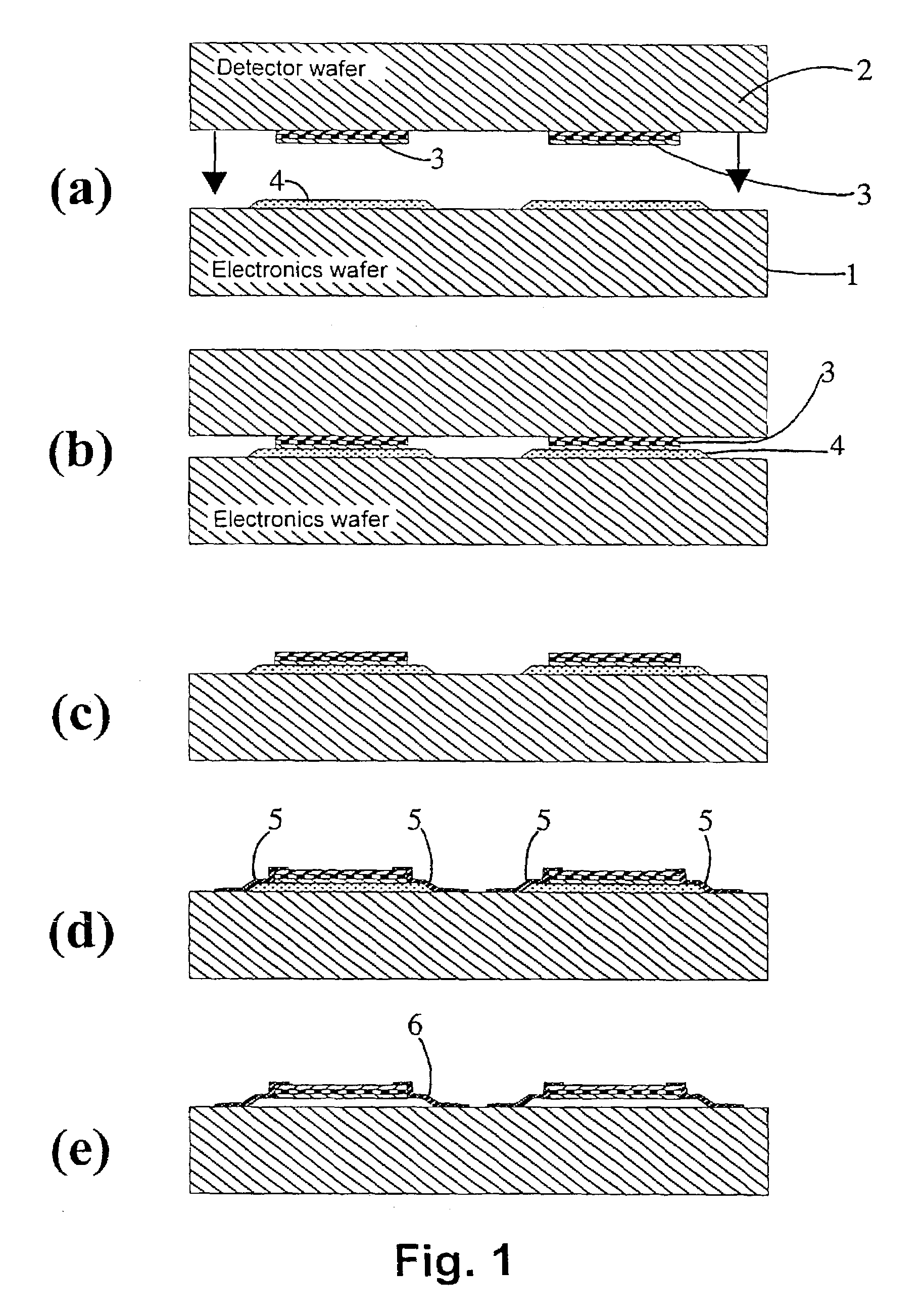
[0009]A great advantage with the inventive method is that the separate structures (detectors and electronics) can be manufactured separately without the over all process being limited by the process parameters for the manufacture of any of the devices. Another advantage is that unique layer sequences, heretofore unattainable can be achieved.
[0011]For a good performance of the detectors it is necessary to use thermistor materials with a high temperature coefficient and low noise. Some of the potential thermistor materials have better material properties when they are deposited at high temperatures (between 500 and 1000° C.). It could also be desired to make the temperature sensing part (thermistor material) of the detector out of a GaAs / AlGaAs epitaxial layer or other materials (for better functionality of the detectors due to better material properties). The epitaxial layer for example can only be deposited and patterned on a GaAs wafer, which requires a transferring technology from the GaAs wafer to the ROIC. Also monocrystaline silicon is due to its material properties potentially a good thermistor material. It is available in good quality only as a bulk material.
[0013]The method according to the invention for transferring structures from one wafer to another, makes it possible to manufacture detectors or parts of them from materials that could not be used so far as detector materials.

Problems solved by technology

A disadvantage is that there is a very restricted selection of materials and methods that are usable for the manufacturing of the detectors, because there is an upper temperature limit of about 400° C., above which the electronic will be damaged.
This makes the manufacturing of detectors having optimal performance more difficult.
A disadvantage is that the IC wafers cannot be manufactured in standard IC foundries, because they have very strict demands on a the process of manufacturing to be standardized in order to be able to maintain the quality in the processes.

Method used


Image

  • Method of joining components
  • Method of joining components
  • Method of joining components

Examples


example 1 (the process of fig.2)

Example 1 (the Process of FIG. 2)

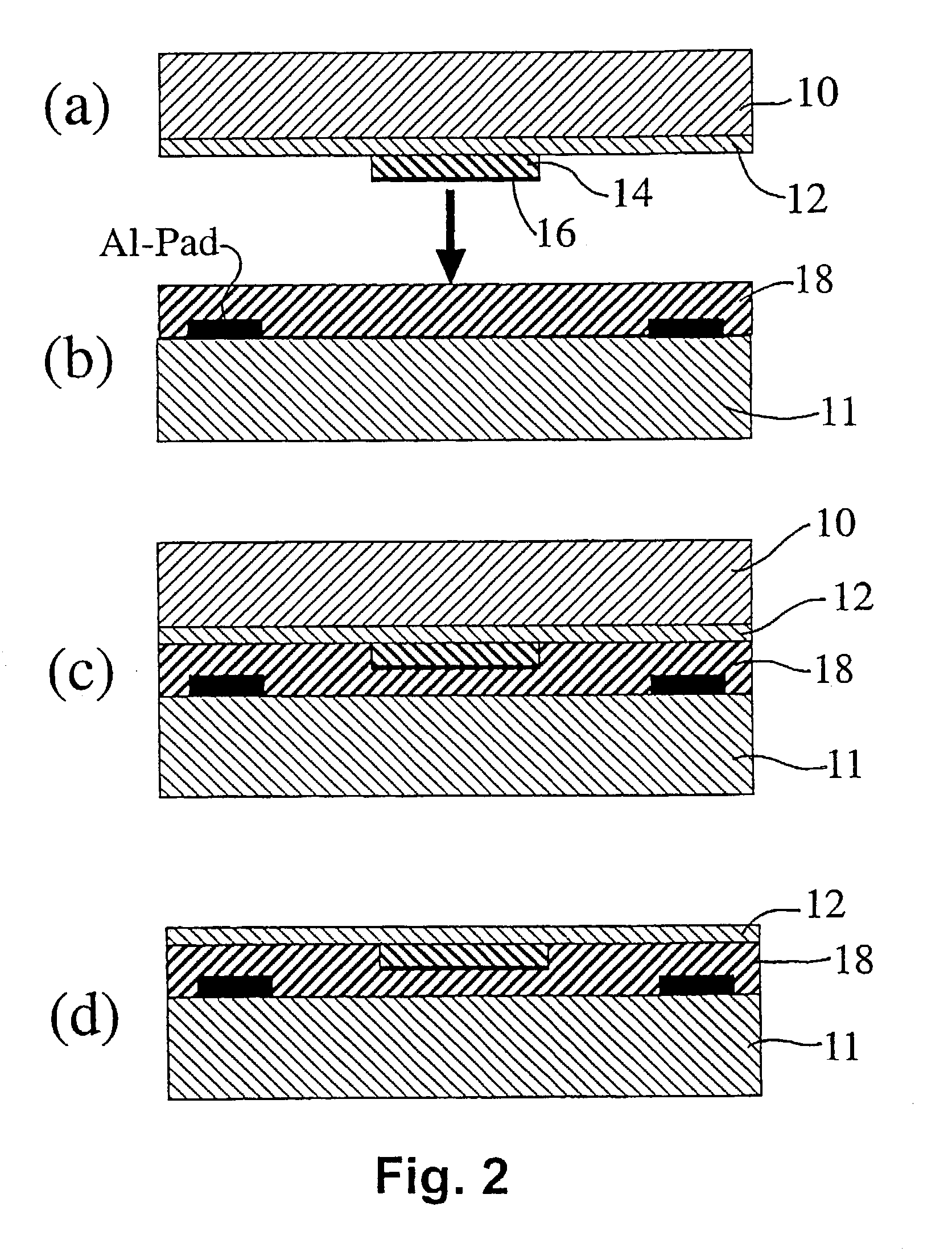
[0034]A silicon wafer 10 is oxidised in an oxidising furnace so that a 1 μm SiO2 layer 12 is produced on its surface. Then a poly-silicon layer 14 of 1 μm thickness is grown on the wafer in a high temperature furnace. A Ti / Pt (50 / 300–500 Å) layer 16 is deposited on the poly-silicon.

[0035]After that, photoresist is spun on the wafer and patterned with photolithography. Then, first the Ti / Pt and subsequently the poly-silicon is etched down to the SiO2 layer with deep reactive ion etching. After stripping of the photoresist the poly-silicon islands remain on the wafer surface (a). The poly-silicon and the SiO2 on the backside of the wafer is etched away with reactive ion etching, so that the backside material of the wafer will be only silicon bulk material. In a next step, first a bonding material 18, e.g. a photo resist, is spun on a ROIC wafer 11, and precured on a hotplate (60° C.) for about 5 min, (b). Then the two wafers are bonded together with a ...

example 2 (process of figs.34 , 57 , 8 and figs.6 , 711 , 12)

Example 2 (Process of FIGS. 34, 57, 8 and FIGS. 6, 711, 12)

[0036]FIG. 3(a) is a top view showing how the cross sections B—B in (b)–(d) are taken. A silicon wafer 40 is oxidised in an oxidising furnace so that a 1 μm SiO2 layer 42 is produced on its surface. Then a poly-silicon layer of 1 μm thickness is provided on the wafer. A Ti / Pt (50+300 Å) layer 44 is deposited on the poly-silicon and patterned with a so called lift-off (FIG. 3(b)). The structures of the Ti / Pt represents the bolometer structures including the bolometer legs. Then a layer 46 of 0.5 μm PE-SiN is deposited on top of the Ti / Pt and polysilicon.

[0037]If for example AlGaAs is used instead of poly-silicon (FIG. 4 showing a similar sequence as in FIG. 3) there needs to be a trench 48, in the temperature sensing material because the resistance of AlGaAs is different in different directions inside the material. In that case the AlGaAs is etched down to the etch stop layer using the Ti / Pt as a mask, before depositing the P...

example 3 (process of fig.5)

Example 3 (Process of FIG. 5)

[0041]A silicon wafer is oxidised in an oxidising furnace so that a 1 μm SiO2 layer is produced on is surface. Then a poly-silicon layer of 1 μm thickness is grown on the wafer in a high temperature furnace. The poly-silicon and the SiO2 on the backside of the wafer is etched with reactive ion etching so that the backside material of the wafer is silicon bulk material.

[0042]A Ti / Pt (50+300 Å) layer is deposited on the poly-silicon and patterned with a so called lift-off. The structures of the Ti / Pt represents the bolometer structures Then a 0.5–4 μm “sacrificial” layer of polyimide is spun on the wafer (on top of the Ti / Pt pattern) and cured.

[0043]Small areas of the polyimide are opened over the Ti / Pt structures. This is done in a way that the polyimide gets sloped walls on this openings. With an other lift-off a second layer of Ti / Pt is patterned on the polyimide representing the leg structures of the detector. The sloped walls of the polyimide guarante...


PUM

PropertyMeasurementUnit
Temperatureaaaaaaaaaa
Structureaaaaaaaaaa
Electrical conductoraaaaaaaaaa

Abstract

A method of combining components to form an integrated device, wherein the components are provided on a first sacrificial wafer, and a second non-sacrificial wafer, respectively. The sacrificial wafer carries a first plurality of components and the non-sacrificial wafer carries a second plurality of components. The wafers are bonded together with an intermediate bonding material. Optionally the sacrificial wafer is thinned to a desired level. The components of the sacrificial wafer are electrically interconnected to the component(s) on the non-sacrificial wafer. Finally, optionally the intermediate bonding material is stripped away.

Description

[0001]The present invention relates to generally to a method of manufacturing an integrated micro electronic device (e.g. a semi-conductor device), comprising transferring structures from a first substrate (e.g. a wafer) to another substrate (e.g. wafer), each substrate comprising components that have been manufactured separately. In particular it relates to a method for integrating transducers on read-out-circuits (ROIC).BACKGROUND OF THE INVENTION[0002]In planar, wafer based mass production of IR detector matrices (hereinbelow referred to as “detectors”) having read-out electronics (hereinbelow referred to as “IC” or “electronics”), two main principles have bee employed.[0003]1. The IC is manufactured to a finished state, and then the detector is manufactured on the IC. The detectors are built onto the IC wafers, an advantage with this approach is that so called IC-foundries can be used, which represents a very cost efficient manufacturing of the electronics wafers. A disadvantage...

Claims


Application Information

Patent Timeline
IPC IPC(8): H01L21/30G01J1/02G01J5/02H01L21/20H01L21/60H01L21/68H01L21/98H01L25/16H01L27/14H01L37/00
CPCH01L21/6835H01L24/24H01L24/82H01L25/50H01L21/2007G01J5/02Y10T156/1092H01L25/16H01L2221/68359H01L2221/68363H01L2224/24011H01L2224/24226H01L2924/01002H01L2924/01013H01L2924/01042H01L2924/01057H01L2924/01077H01L2924/01078H01L2924/10329H01L2924/10336H01L2924/1433H01L2924/01005H01L2924/01006H01L2924/01033H01L2924/01072
Inventor KALVESTEN, EDVARDSTEMME, GORANNIKLAUS, FRANK
Owner FAUN DATA
Learn More