MOSFET with short channel structure and formation method thereof

a technology of mosfet and short channel, which is applied in the direction of basic electric elements, electrical apparatus, and semiconductor devices, can solve the problems of bringing additional cost and complexity during processing, and the mosfet performance is not good when the gate is turned, so as to reduce the effect of short channel, and reduce the resistance to increase the operating curren

Inactive Publication Date: 2006-06-13
WINBOND ELECTRONICS CORP
View PDF2 Cites 9 Cited by
  • Summary
  • Abstract
  • Description
  • Claims
  • Application Information

AI Technical Summary

Benefits of technology

[0007]One object of the present invention is to utilize a MOSFET with a short channel structure including lower threshold voltages to replace a source / drain extension. There are three MOSFETs having a variety of threshold voltages to substantially decrease the serial resistance of MOSFETs.
[0011]When a voltage applied to the gate increases, the resistance of the first region is effectively reduced the overall resistance between the source and the drain. If the turn-on voltage is higher than the threshold voltage of the first region, the first region has a sufficient low resistance. When the gate is turned off, the first region has a very high resistance to reduce leakage current between the source and drain.
[0013]In summary, the present invention provides the MOSFET with a short channel structure. The first region provides a lower resistance to increase an operating current between the source / drain when the gate is turned on. The first region has a very high resistance to substantially decrease the sub-threshold current when the gate is turned off. Moreover, the junction depth of the first region is shallower than that of the conventional source / drain extension to reduce the short channel effects.

Problems solved by technology

However, doping concentration and junction depth of the source / drain extension 106 are lower and shallower, respectively, than those of the source / drain 102, which lead to worse performance of the MOSFET when the gate is turned on.
Therefore, to obtain a shallow junction depth in the source / drain extension 106, many doping and annealing steps tightly controlled bring additional cost and complexity during processing.
Consequently, how to improve device performance due to a high resistance in the source / drain extension is an important problem and is currently a main issue for semiconductor manufacturers.

Method used


Image

  • MOSFET with short channel structure and formation method thereof
  • MOSFET with short channel structure and formation method thereof
  • MOSFET with short channel structure and formation method thereof

Examples


Embodiment Construction

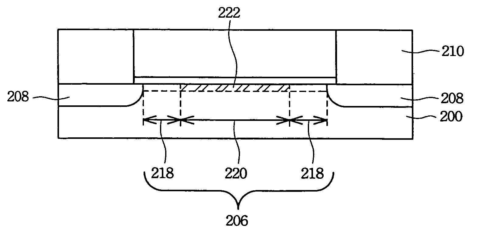
[0017]The present invention is directed to a MOSFET with a short channel structure to improve the shortcomings of a MOSFET used in the prior art. The present invention is suitable for an NMOS and a PMOS transistor. To illustrate the present invention, an example of the NMOS is set forth in details as follows.

[0018]FIGS. 2A–2K show process cross-sectional views of a MOSFET with a short channel structure according to the present invention. In FIG. 2A, performing a first ion implantation 202 on a substrate 200 obtains a doping concentration of a first threshold voltage, in which the first threshold voltage can be changed with the doping concentration. In the preferred embodiment of the present invention, the dopant of the first ion implantation 202 includes boron (B) which has an implanting energy range of about 5 to 70 keV and an doping concentration range of about 1×1012 cm−2 to 3×1013 cm−2.

[0019]Afterwards, a sacrificial layer 204 is formed on the substrate 200. For example, the for...


PUM


Abstract

A MOSFET with a short channel structure and manufacturing processes for the same are described. The MOSFET has a substrate, a channel region, a source / drain region, a gate dielectric layer and a conductive layer. The channel region in the substrate includes a first region and a second region, in which the first region has a first threshold voltage and the second region has a second threshold voltage, respectively. The first threshold voltage is smaller than the second threshold voltage. The first threshold voltage of the first region can also be adjusted to reduce or increase effectively the resistance of the MOSFET when the MOSFET is turned on or off. Additionally, the first region has a shallower junction depth than that of the normal source / drain extension.

Description

CROSS-REFERENCE TO RELATED APPLICATIONS[0001]This application is a divisional of U.S. patent application Ser. No. 10 / 244,535, filed Sep. 17, 2002, now abandoned.FIELD OF THE INVENTION[0002]The present invention generally relates to semiconductor structures and processes, and more particularly, to a MOSFET with a short channel structure and manufacturing method.BACKGROUND OF THE INVENTION[0003]With the rapid increment of integration and operating frequency of integrated circuits (ICs), the size of the IC must shrunk to meet the requirements of the semiconductor industry. A source / drain extension, a gate length, and junction depth of the source / drain particularly need to be diminished to solve the problems of process complexity and severe short channel effects.[0004]To solve the problem of the short channel effects, a junction depth reduction of the source / drain extension has been developed. FIG. 1 shows a cross-sectional view of a conventional MOSFET. A source / drain 102 is formed on ...

Claims


Application Information

Patent Timeline
Patent Type & Authority Patents(United States)
IPC IPC(8): H01L21/336H01L21/265H01L29/10
CPCH01L29/66545H01L29/1045H01L21/26513
Inventor JANG, WEN-YUEH
Owner WINBOND ELECTRONICS CORP
Why Eureka
Try Eureka