Mold component and mold assembly

a mold and component technology, applied in the field of mold components and mold assemblies, can solve the problems of uneven thickness of resin r and formation of coating streaks, reduced outer diameter of stampers, and difficulty in completely preventing the occurrence of the above inconvenience, and achieve uniform thickness

Active Publication Date: 2006-05-16
TDK CORPARATION
View PDF4 Cites 16 Cited by
  • Summary
  • Abstract
  • Description
  • Claims
  • Application Information

AI Technical Summary

Benefits of technology

[0013]The present invention has been made in view of the above-described point to be improved, and it is a main object of the invention to provide a mold component and a mold assembly which make it possible to mold a substrate for an optical recording medium which enables a functional layer having a uniform thickness to be formed thereon without using a resin-coating assisting member.
[0015]According to the mold component and the mold assembly, through a central portion of the stamper, there is formed an insertion hole having a diameter which is larger than an outer diameter of a cavity-side end of the stamper holder, at a high temperature, and is reduced to be slightly smaller than the outer diameter at a normal temperature. The cavity-side end of the stamper holder inserted into the insertion hole of the stamper at the higher temperature is grasped by a rim of the insertion hole which is reduced in diameter at the normal temperature, to cause the stamper holder to hold the stamper thereon. As a result, a holding piece of the stamper holder for holding the stamper can be dispensed with, and hence it is possible to positively prevent a groove from being formed due to the projection of the holding piece in molding the substrate. Therefore, the resin can be dropped onto the central portion of the substrate, e.g. by forming the substrate such that it has a central hole having a small diameter. This makes it possible to form a functional layer having a uniform thickness on the substrate without using a resin-coating assisting member.
[0016]Preferably, the stamper holder is configured such that the outer diameter of the cavity-side end thereof is smaller than an outer diameter of an end of the stamper holder opposite to the cavity-side end. According to this configuration, when the stamper holder is inserted into the insertion hole of the stamper, a stepped portion is brought into abutment with the rim of the insertion hole, which makes it possible to insert the stamper holder into the insertion hole, while accurately positioning the stamper holder.
[0017]Preferably, the mold assembly further comprises a sprue bushing disposed in the first mold, and having the stamper holder mounted on an outer periphery thereof, and a cavity-side end face of the stamper holder is slightly protruded toward the cavity with respect to a cavity-side end face of the sprue bushing, while the molding surface of the stamper is slightly protruded toward the cavity with respect to the cavity-side end face of the stamper holder. According to this configuration, it is possible to prevent a gap from being formed between the stamper and the stamper holder, whereby burrs can be prevented from being formed during molding. Further, the substrate for an optical recording medium can be formed such that a surface of the substrate becomes slightly lower in level toward the radially outer side, which enables the resin to be drawn smoothly. Further, it is possible to prevent formation of an annular groove, thereby enabling the resin to be drawn more smoothly. This makes it possible to coat the resin having a substantially uniform thickness without unevenness.

Problems solved by technology

Therefore, when the resin R is coated on the one surface of the molded substrate D4 by the spin coating method, the annular groove D4d impedes the smooth drawing of the resin R, which can cause defects, such as uneven thickness of the resin R and formation of coating streaks.
However, since there is a limit to reduction of the outer diameter of the stamper, it is difficult to completely prevent the occurrence of the above inconvenience by the above method.
This presents a hurdle in employing the method.

Method used


Image

  • Mold component and mold assembly
  • Mold component and mold assembly
  • Mold component and mold assembly

Examples


Embodiment Construction

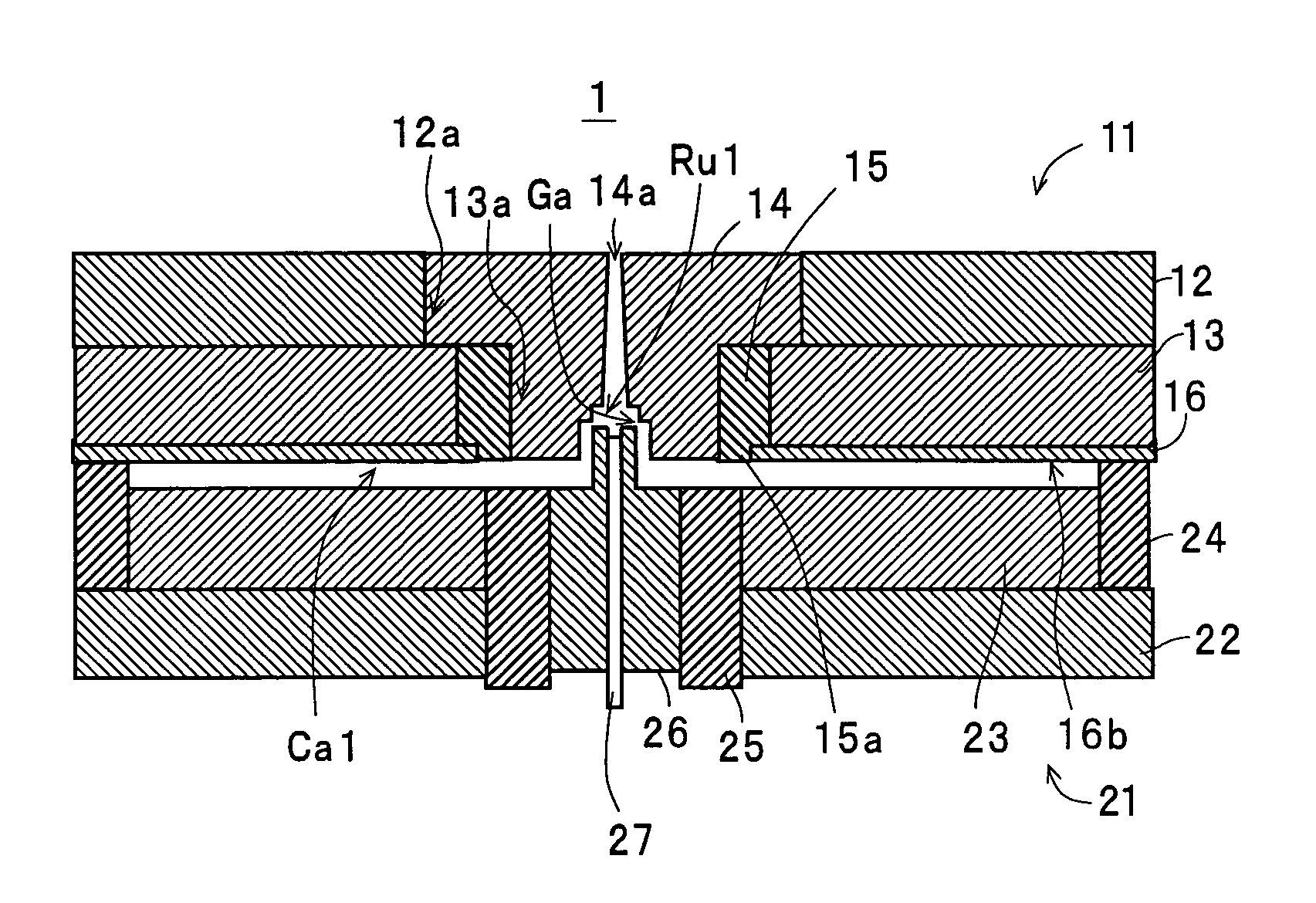
[0035]The invention will now be described in detail with reference to the drawings showing preferred embodiments thereof. It should be noted that the component parts and elements identical to those of the conventional mold assembly 51 are designated by identical reference numerals and detailed description thereof will be omitted.

[0036]First, the construction of a mold assembly 1 will be described with reference to drawings.

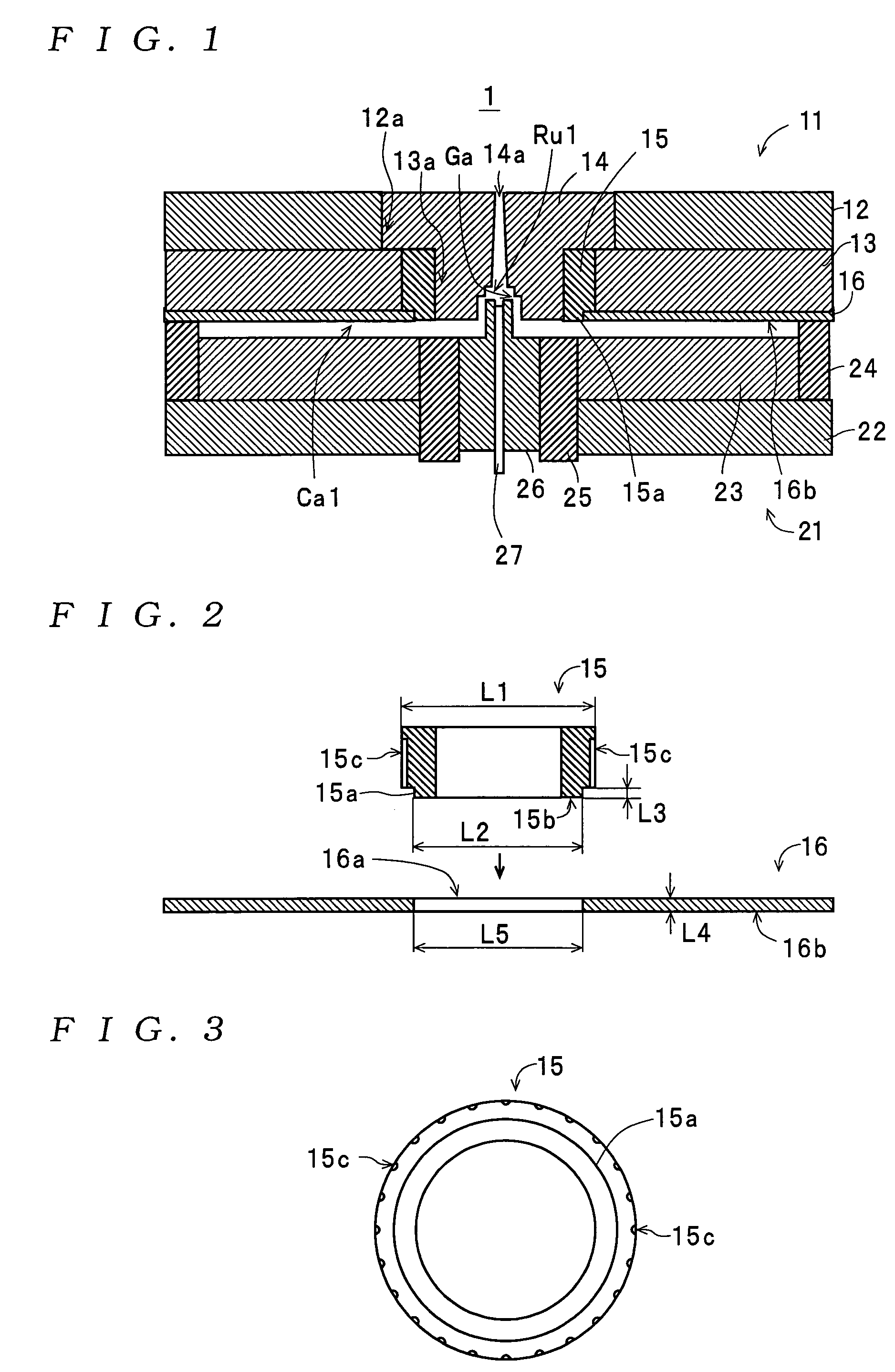
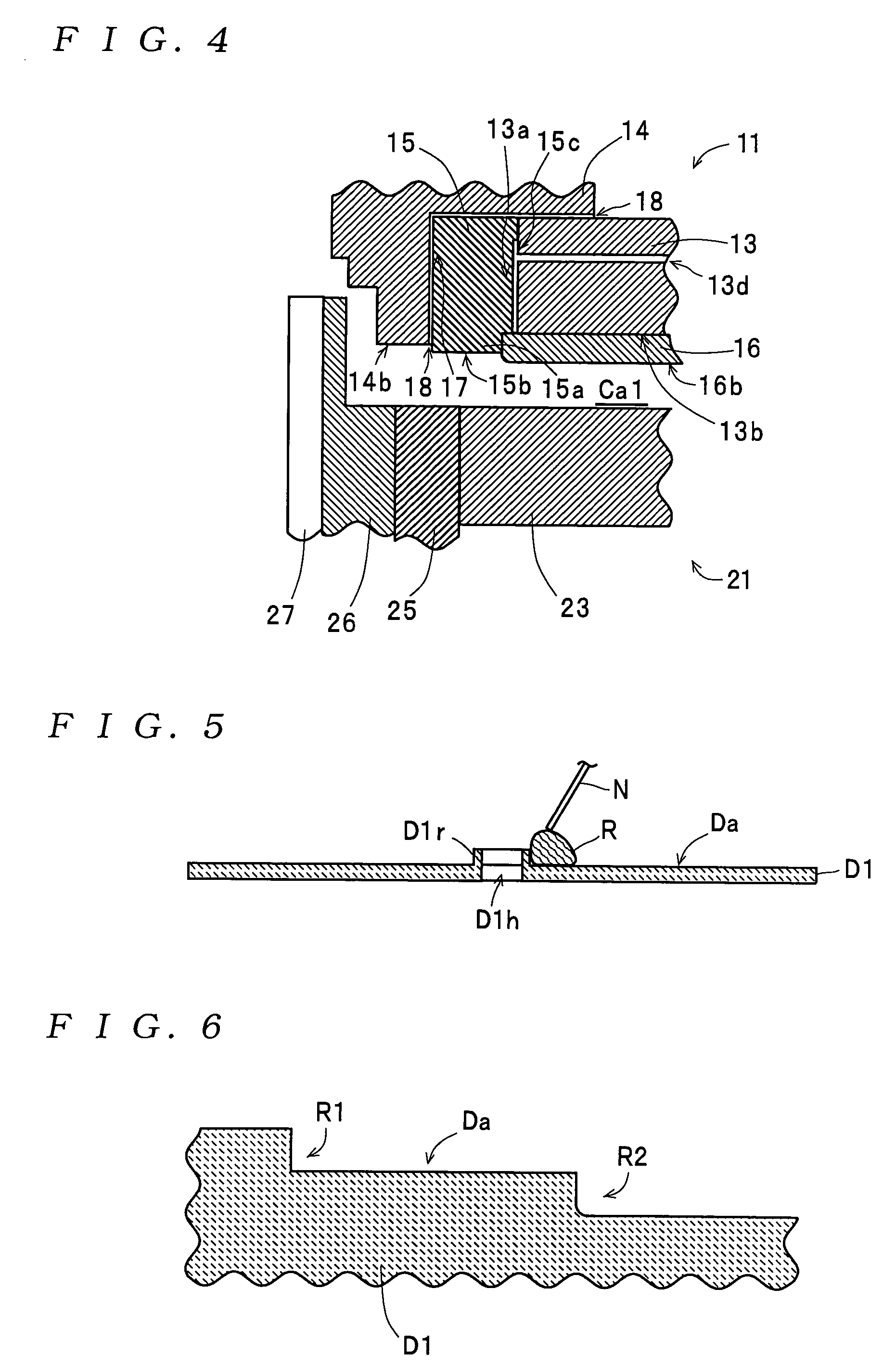
[0037]Referring first to FIG. 1, the mold assembly 1 is comprised of a fixed mold (first mold) 11, and a movable mold (second mold) 21 which can move to and away from the fixed mold 11. Further, the mold assembly 1 is configured such that a substrate D1 for an optical recording medium (hereinafter simply referred to as “the substrate D1”) formed with a central hole D1h and a hollow cylindrical protruding portion D1r, as shown in FIG. 5, can be molded by causing an injection molding apparatus, not shown, to inject a molten resin material into a cavity Ca1 formed by...


PUM

PropertyMeasurementUnit
Diameteraaaaaaaaaa
Heightaaaaaaaaaa

Abstract

There is provided a mold component which makes it possible to mold a substrate for an optical recording medium which enables a functional layer having a uniform thickness to be formed thereon without using a resin-coating assisting member. A stamper holder holds a stamper thereon, and has a generally hollow cylindrical shape. An insertion hole formed through a central portion of the stamper has a diameter which is larger than an outer diameter of a cavity-side end of the stamper holder at a higher temperature of the holder than a normal temperature, and is slightly smaller than the outer diameter at the normal temperature of the holder. The cavity-side end inserted into the insertion hole at the higher temperature of the stamper is grasped by a rim of the insertion hole which is reduced in diameter at the normal temperature of the stamper.

Description

BACKGROUND OF THE INVENTION[0001]1. Field of the Invention[0002]This invention relates to mold components and a mold assembly, for molding a substrate for an optical recording medium.[0003]2. Description of the Related Art[0004]Conventionally, as a mold assembly for molding a substrate D3 (see FIG. 15) for an optical recording medium, such as a CD (Compact Disc) and a DVD (Digital Versatile Disc), a mold assembly has been known which includes a fixed mold having a stamper set thereon for forming micro asperities, such as grooves, in a surface of the substrate D3, and a movable mold having a sleeve set therein for forming a central hole D3h (central hole for mounting the optical recording medium) in the substrate D3. As shown in FIG. 15, the substrate D3 molded using the mold assembly has the central hole D3h formed in a central portion thereof, and micro asperities, such as grooves, not shown, formed in a predetermined area on one surface (upper surface, as viewed in FIG. 15) thereo...

Claims


Application Information

Patent Timeline
IPC IPC(8): B29D11/00B29C45/36B29C45/00B29C45/26B29D17/00B29L17/00G11B7/26
CPCB29C45/0053B29C45/2632B29D17/005B29C2045/0079Y10S425/81B29L2017/003B29C2045/264
Inventor KOYAMA, ATSUSHIUSAMI, MAMORUYAMAGA, KENJIDOMON, MIKIOSUZAWA, KAZUKI
Owner TDK CORPARATION
Why Eureka
Try Eureka