Method for manufacturing metal thin film resistor
a technology of resistor and metal thin film, which is applied in the direction of resistor details, resistors adapted for applying terminals, resistive material coatings, etc., can solve the problems of metal thin film deterioration, excessive surface treatment process, and lowering yield, so as to improve the response characteristic of the device formed, improve the thermal conductivity of the substrate and the response characteristic of the thermosensor, and improve the effect of line width control
- Summary
- Abstract
- Description
- Claims
- Application Information
AI Technical Summary
Benefits of technology
Problems solved by technology
Method used
Image
Examples
embodiment 1
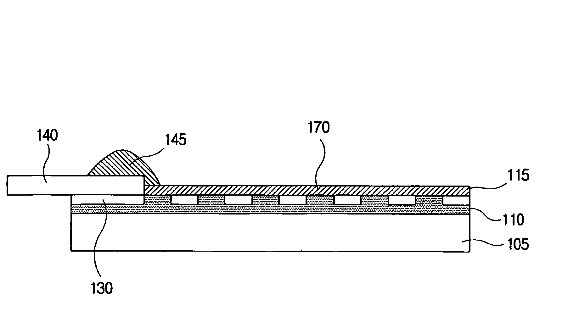
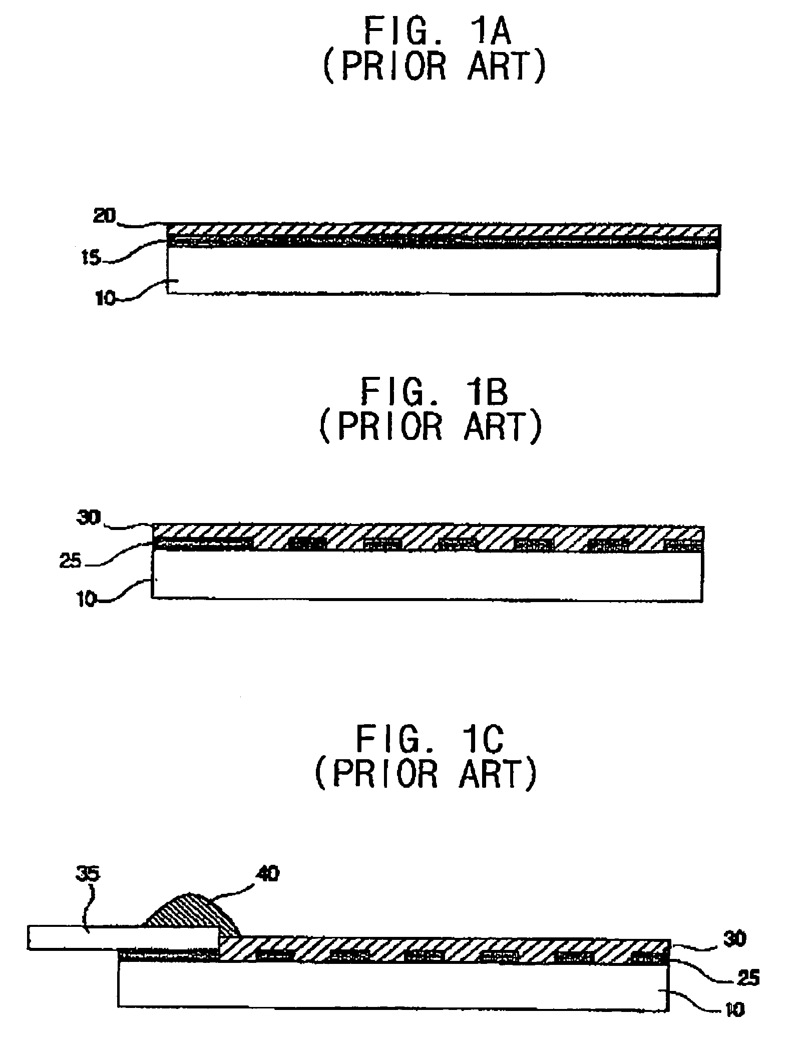
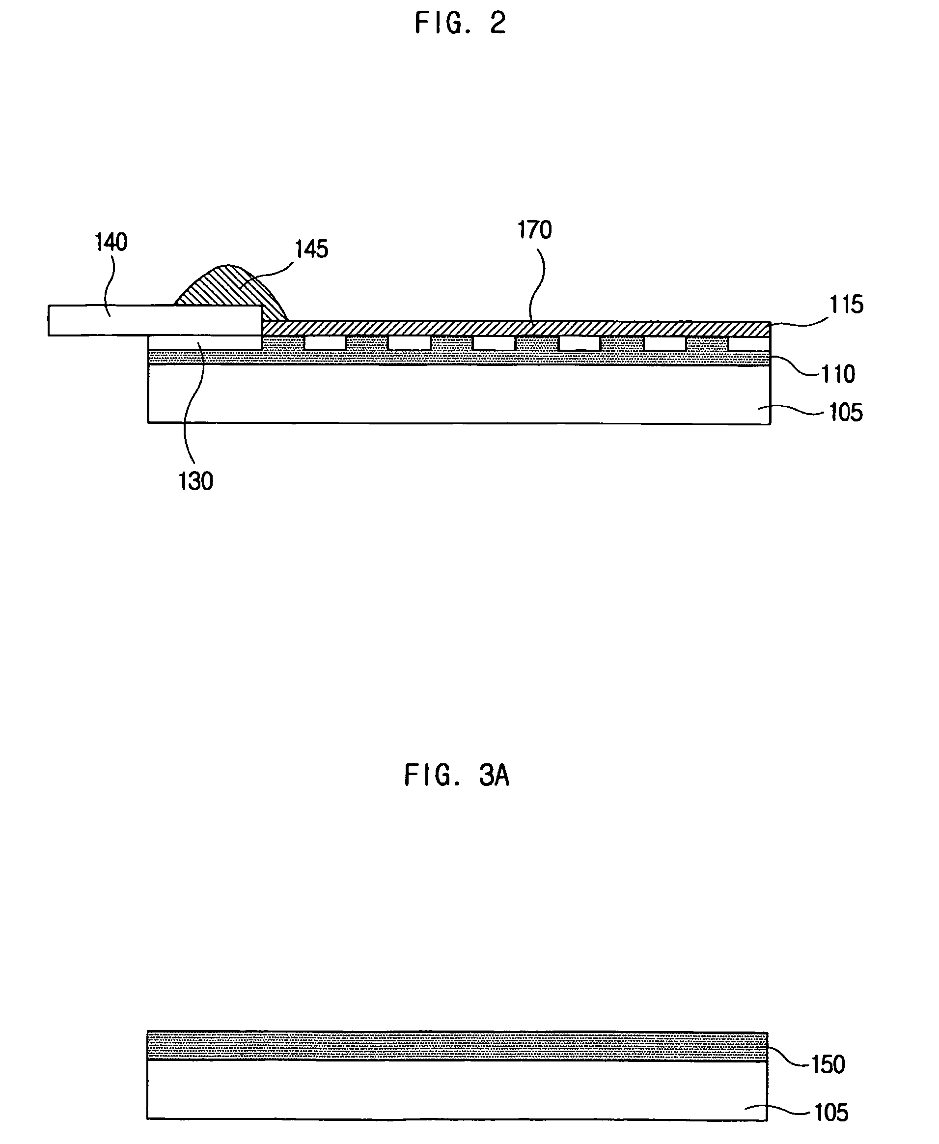
[0064]At first, after a thermal oxidation film corresponding to a first insulation film was formed on a substrate such as a silicon wafer to have a thickness of about 2.5 μm by the thermal oxidation method, a photosensitive film was coated on the thermal oxidation film. Then, the thermal oxidation film was patterned by the photolithography process to form insulation film patterns having line width of about 0.1˜2 μm. The insulation film pattern on the substrate has a thickness of about 1.5 μm. When the thermal oxidation film was patterned, a BOE solution was used as an etchant widly used in semiconductor technology.
[0065]Platinum was sputtered to from a platinum thin film having a thickness of about 1.0 μm while the photosensitive film was coated on the insulation film patterns. The platinum thin film was formed using a platinum target having a purity of above 99.995% and a size of about 4 inched at a room temperature under a deposition pressure of about 1˜10 mTorr with a deposition ...
embodiment 2
[0069]A test wafer for compensating temperature used in semiconductor manufacturing process was manufactured according to the present embodiment.
[0070]At first, after an oxide film corresponding to a first insulation film was formed on a substrate such as a silicon wafer to have a thickness of about 3.5 μm by the thermal oxidation method, a photosensitive film was coated on the oxide film. Then the oxide film was patterned by the photolithography process, thereby forming insulation film patterns having line widths of about 1.0 μm and thicknesses of about 1.5 μm on the substrate. When the oxide film was patterned, the BOE solution was used as an etchant widely used in the semiconductor technology.
[0071]A platinum thin film having a thickness of approximately 1.0 μm was formed by sputtering platinum on the insulation film patterns and on the photosensitive film. At that time, the processing conditions for forming the platinum thin film were identical to those of the aforementioned emb...
embodiment 3
[0073]After an oxide film as a first insulation film was formed on a substrate such as a silicon wafer to have a thickness of about 3.5 μm by the thermal oxidation method, a photosensitive film was coated on the oxide film. Then, the oxide film was patterned by the photolithography method, so that insulation film patterns having line widths of about 2 μm and thicknesses of about 1.5 μm. When the oxide film was patterned, a BOE solution was used as an etchant used in the semiconductor technology. A negative or a positive photosensitive film can be used as the photosensitive film in accordance with the process for forming the insulation film patterns.
[0074]While the photosensitive film is coated on the insulation film patterns, a platinum thin film having a thickness of about 1.0 μm was formed by sputtering platinum on the photosensitive film and on the insulation film patterns. Preferably, the platinum thin film was deposited using a platinum target having a purity of above 99.995% a...
PUM
| Property | Measurement | Unit |
|---|---|---|
| widths | aaaaa | aaaaa |
| thickness | aaaaa | aaaaa |
| size | aaaaa | aaaaa |
Abstract
Description
Claims
Application Information
 - R&D
- Intellectual Property
- Life Sciences
- Materials
- Tech Scout
- Unparalleled Data Quality
- Higher Quality Content
- 60% Fewer Hallucinations
Browse by: Latest US Patents, China's latest patents, Technical Efficacy Thesaurus, Application Domain, Technology Topic, Popular Technical Reports.
© 2025 PatSnap. All rights reserved.Legal|Privacy policy|Modern Slavery Act Transparency Statement|Sitemap|About US| Contact US: help@patsnap.com


