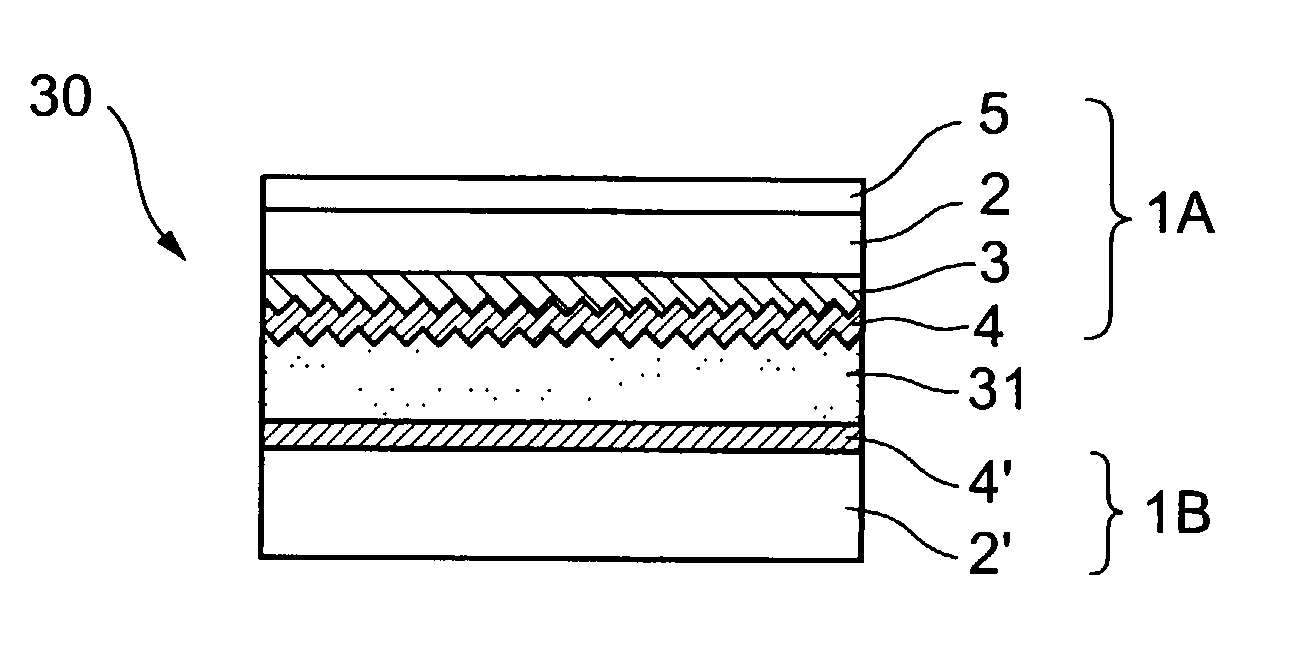
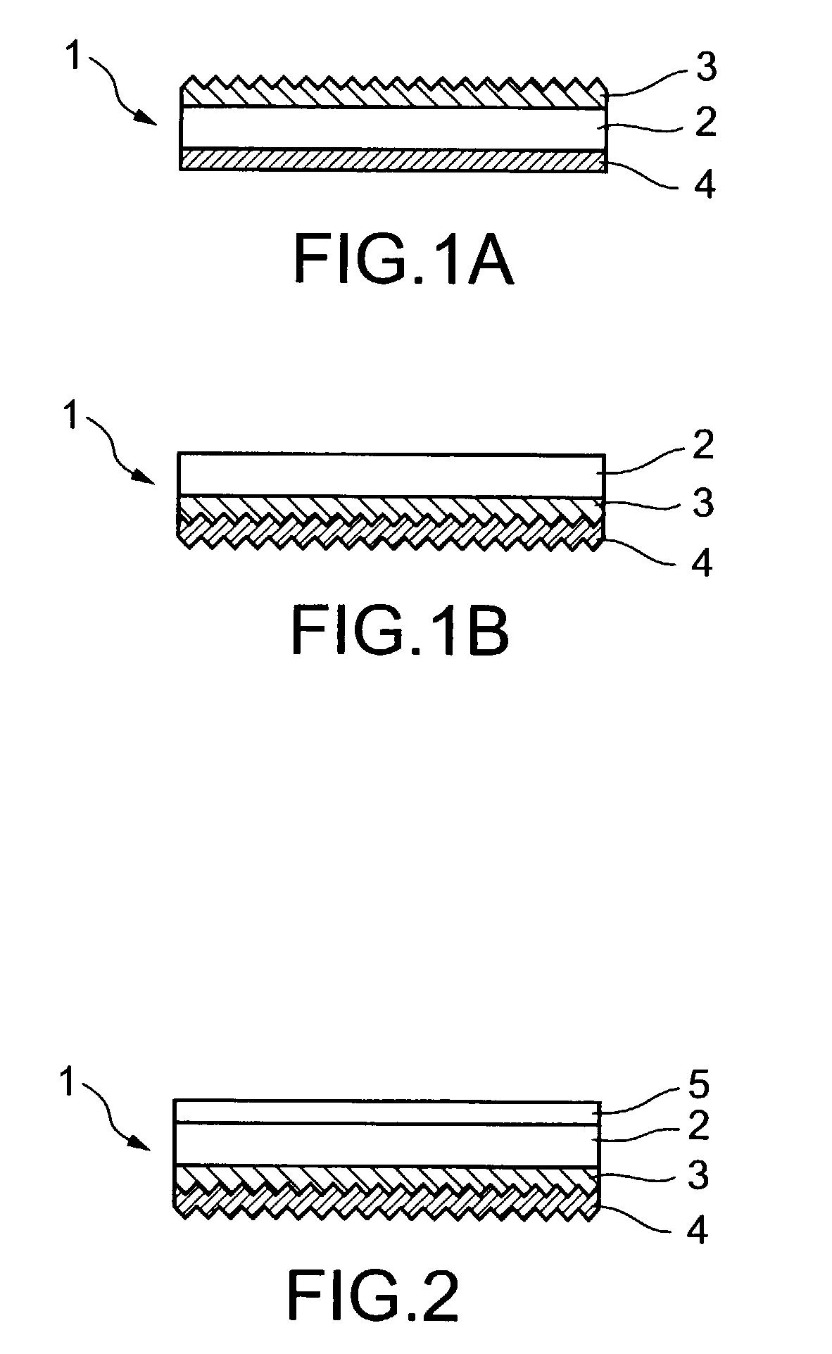
Transparent conductive film
a technology of transparent conductive film and mirror surface, which is applied to the conductive layers on the insulating support, identification means, instruments, etc., can solve the problems of substrate sticking, poor surface slipperiness, and substrate blockage, etc., and achieve excellent slipperiness, good slipperiness, and easy production of touch panels
- Summary
- Abstract
- Description
- Claims
- Application Information
AI Technical Summary
Benefits of technology
Problems solved by technology
Method used
Image

Examples
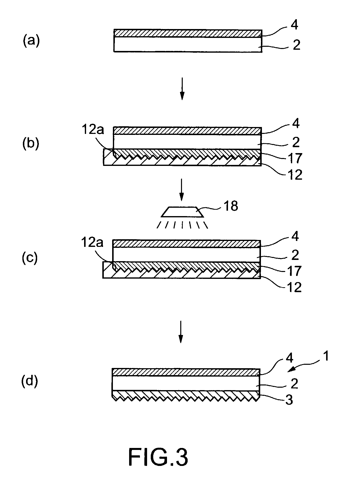
example 1
[0108]200-mesh glass beads (particle diameter: approximately 130 μm) were blown over an iron-made roller by beads shot blasting to form fine irregularities on the surface of the roller. The roller provided with fine irregularities was then plated with chromium so that the thickness of the chromium layer would be 5 μm, thereby obtaining an embossing roller.
[0109]On the other hand, a 188-μm thick polyethylene terephthalate resin film was prepared as the transparent plastic film. A composition consisting of a polyurethane resin primer (manufactured by The Inctec Inc., Japan), and a 10:1:3.3 (weight ratio) mixture of a medium main agent for chemical mat varnish, a curing agent (XEL curing agent) and a solvent was applied to one surface of the transparent plastic film by gravure coating, and was then dried to form a 3-μm thick primer layer. The solvent used was a 1:1 solvent mixture of toluene and methyl ethyl ketone. It is noted that all blend ratios that appear in the descriptions of E...
example 2
[0112]The procedure of Example 1 was repeated to obtain a transparent conductive film, provided that a 100:75 (weight ratio) mixture of an ultraviolet-light-curing acrylic resin (trademark “PET-D31”, manufactured by Dainichiseika Color & Chemicals Mfg. Co., Ltd., Japan) and a solvent was applied by roll coating (twin reverse rolls) to the surface of the polyethylene terephthalate resin film to which the transparent resin layer having fine irregularities and the ITO thin film had not been laminated, was dried, and was then cured by the application of ultraviolet light to form a hard coat layer having a mirror surface. The solvent used was a 3:1 mixture of toluene and methyl ethyl ketone.
PUM
| Property | Measurement | Unit |
|---|---|---|
| height | aaaaa | aaaaa |
| mean roughness | aaaaa | aaaaa |
| mean roughness | aaaaa | aaaaa |
Abstract
Description
Claims
Application Information
 - R&D
- Intellectual Property
- Life Sciences
- Materials
- Tech Scout
- Unparalleled Data Quality
- Higher Quality Content
- 60% Fewer Hallucinations
Browse by: Latest US Patents, China's latest patents, Technical Efficacy Thesaurus, Application Domain, Technology Topic, Popular Technical Reports.
© 2025 PatSnap. All rights reserved.Legal|Privacy policy|Modern Slavery Act Transparency Statement|Sitemap|About US| Contact US: help@patsnap.com