
Co-packaged control circuit, transistor and inverted diode

a control circuit and inverter diode technology, applied in the direction of semiconductor devices, semiconductor device details, electrical apparatus, etc., can solve the problems of limited thermal management of power switch b>10/b>, substantial electrical connection space for components in electronic circuits, etc., to reduce the number of external leads for connecting to a circuit board, such as a pcb, and reduce the size of a power factor correction circuit.

Inactive Publication Date: 2005-12-13
INFINEON TECH AMERICAS CORP
View PDF4 Cites 34 Cited by
  • Summary
  • Abstract
  • Description
  • Claims
  • Application Information

AI Technical Summary

Benefits of technology

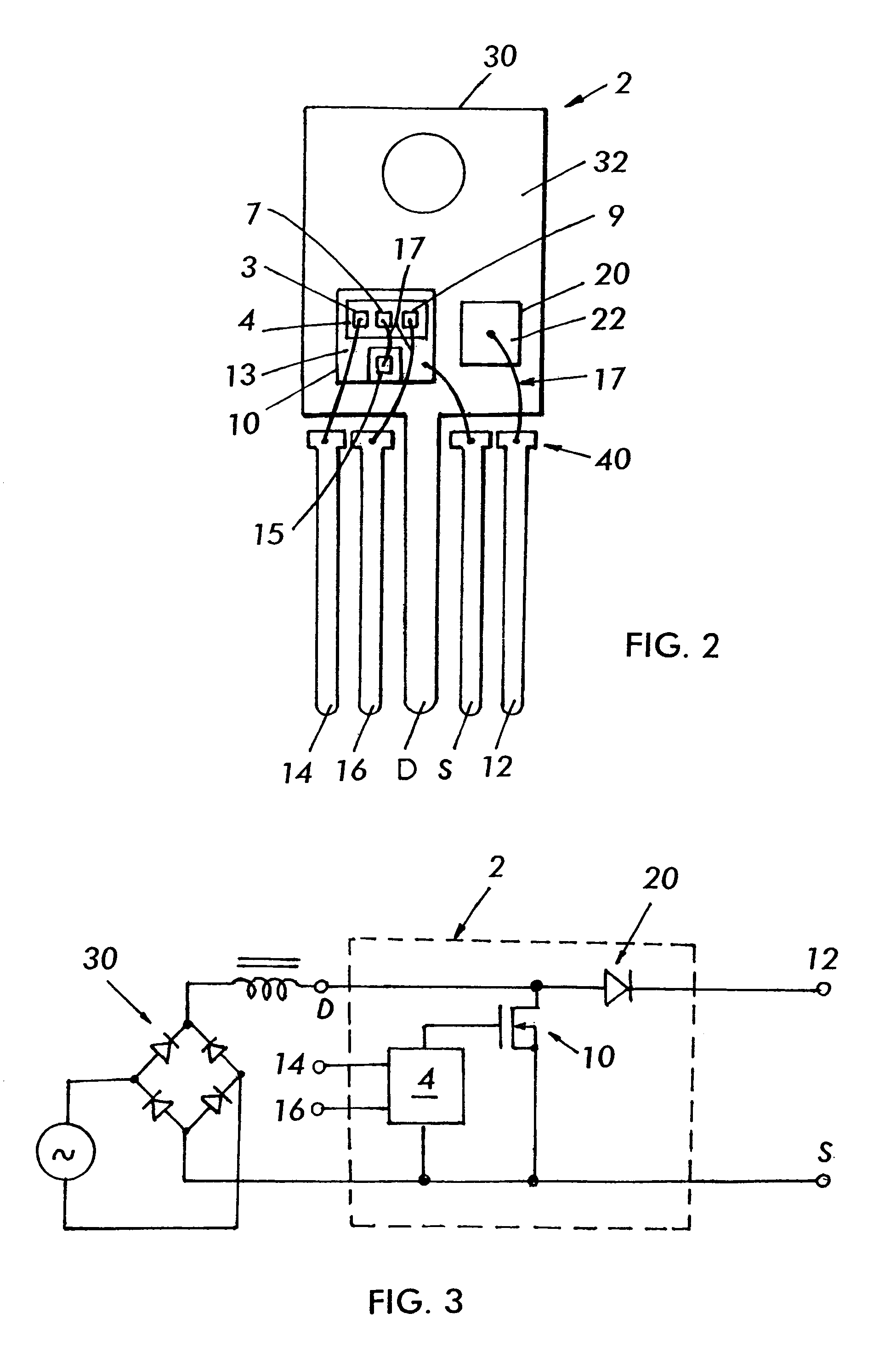
[0008]In one example, a copackaged electronic device is packaged in a power package, such as a TO220, D2pak, TO220FP or TO247, while including the control circuit and the power switching device together with the diode. The number of discrete parts, the number of individual connectors, and the number of wire bonds or wire traces between components are reduced compared to conventional use of discrete components of an AC to DC converter with power factor correction. For example, a through hole lead frame package may be mounted directly to a heat sink via an exposed back surface of the lead frame pad, greatly improving and simplifying thermal management of the heat generating power switching device and diode.
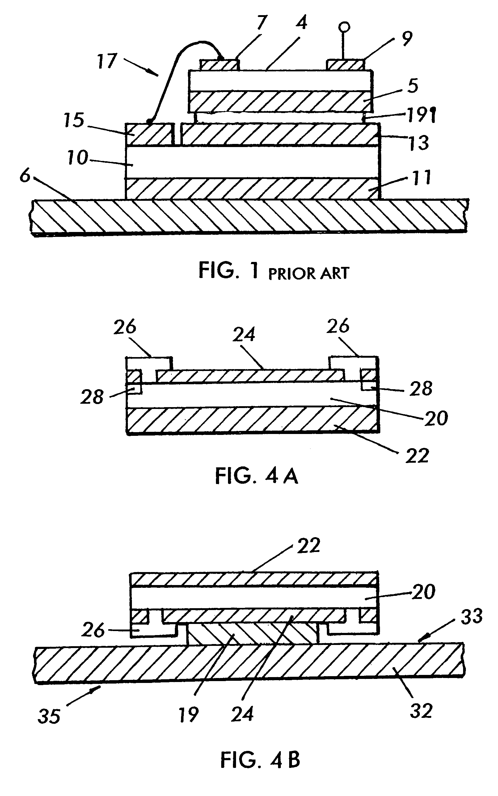
[0010]In one embodiment, a passivation layer surrounds the anode of the inverted diode. The passivation layer protects the termination structure of the inverted diode, allowing the anode to be directly joined to the electrically conductive surface of a die pad. The passivation layer electrically insulates the termination structure from the conductive lead frame.
[0011]One advantage of the copackaged device is that the size of a power factor correction circuit is reduced. Another advantage is that fewer wire bonds are required, reducing circuit resistance and inductance. Yet another advantage is that the number of external leads for connecting to a circuit board, such as a PCB, is reduced compared to a conventionally mounted transistor, integrated circuit controller and diode. Yet another advantage is that thermal management of the heat generating components is simplified and improved by copackaging the power switching device and the diode.

Problems solved by technology

However, a disadvantage of mounting a conventional combined chip directly to a PCB is that thermal management of the power switch 10 is limited by the presence of the PCB adjacent to the combined chip.
However, such an architecture requires inventory and supply management, thermal management and electrical contacts for each of the separately packaged power devices, as both the power switch and the diode produce heat.
Also, separately packaging the components and integrating the components in an electronic circuit requires a substantial amount of space for making electrical connections between the separately packaged component parts.

Method used


Image

  • Co-packaged control circuit, transistor and inverted diode
  • Co-packaged control circuit, transistor and inverted diode
  • Co-packaged control circuit, transistor and inverted diode

Examples


Embodiment Construction

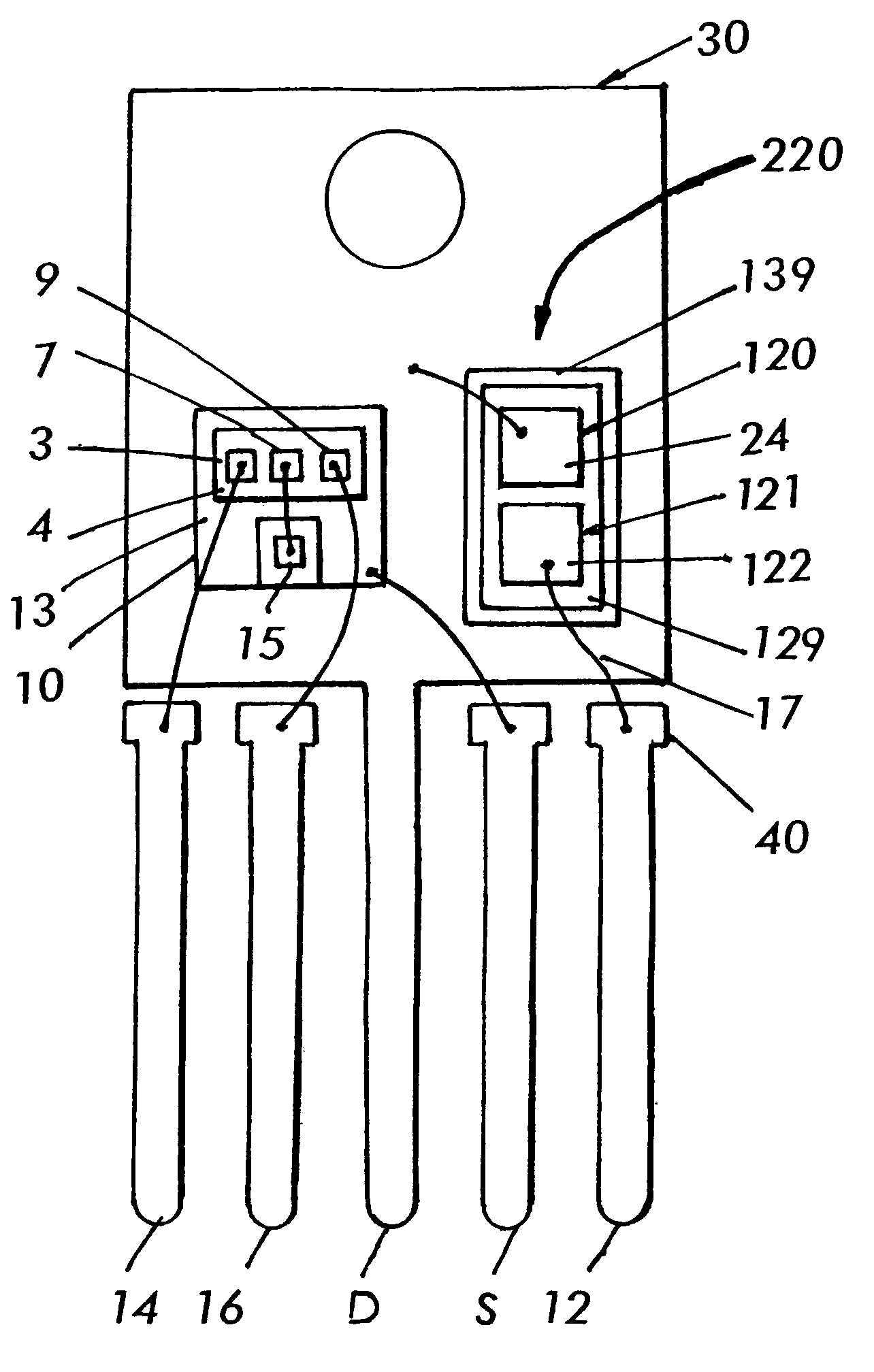
[0022]Now referring to FIG. 2, one embodiment of a copackaged electronic device 2 comprises a single, 600 Volt (V) fast recovery diode 20 electrically connected to the drain electrode 11 of a MOSFET 10 via an electrically conductive pad 32 of a lead frame 30. The diode 20 is laterally removed from the MOSFET 10 on the mounting surface of the pad 32 and the anode electrode 24 of the diode 20 is electrically mounted on the mounting surface of the pad 32. For example, the diode 20 may be a flip chip diode (e.g. inverted), having the cathode electrode 24 of the diode 20 wire bonded 17 to a lead 12 of the lead frame 30. For example, a contact pad 40 electrically couples a wire bond 17 to the lead 12. Flip chip mounting of the diode 20 greatly simplifies the assembly process and reduces the number of wire bonds required, which reduces wire bond resistance and inductance, improving the efficiency of the discrete copackaged electronic device 2 of FIG. 2 compared to devices using a conventio...


PUM


Abstract

A copackaged electronic device comprises a diode device having an anode coupled to a drain electrode of a switching device and a cathode capable of being coupled to an external circuit. The switching device may be controlled by an integrated circuit mounted on a source electrode of the switching device and electrically connected such that the integrated circuit is capable of controlling switching of the switching device. For example, the device is used in a power factor correction circuit. The diode device comprises at least one inverted diode having a solderable anode and a wire-bondable cathode.

Description

RELATED APPLICATION[0001]This application is a continuation-in-part of U.S. application Ser. No. 10 / 377,683 to Stephen Oliver and Hugh D. Richard, entitled “Semiconductor Package for Series-Connected Diodes,” filed Feb. 28, 2003, U.S. Pat. No. 6,740,902 which claims the benefit of U.S. Provisional Application No. 60 / 408,519, filed Sep. 4, 2002, entitled “Tandem Diode Package with One Flip Chip.” The disclosures of Ser. Nos. 10 / 377,683 and 60 / 408,519 are incorporated by reference herein in their entirety.FIELD OF THE INVENTION[0002]The field of the invention is electronic packaging of switching device. Specifically, a diode is copackaged with a power switch and control circuitry.BACKGROUND OF THE INVENTION[0003]As shown in FIG. 1, a combined chip, consisting essentially of a power switch 10, such as a MOSFET, and an integrated circuit control chip 4 mounted directly on a source electrode 13 of the power switch 10 by an adhesive 191, is known. In the example shown in FIG. 1, the adhes...

Claims


Application Information

Patent Timeline
IPC IPC(8): H01L21/60H01L23/495H01L27/15H01L29/00H01L31/12H01L33/00
CPCH01L23/49562H01L23/49575H01L24/33H01L24/49H01L24/83H01L24/45H01L2224/05624H01L2224/291H01L2224/45124H01L2224/45144H01L2224/48091H01L2224/48247H01L2224/49171H01L2224/73265H01L2224/83101H01L2224/8319H01L2224/83801H01L2924/01005H01L2924/01013H01L2924/01027H01L2924/01029H01L2924/01079H01L2924/01082H01L2924/0781H01L2924/13055H01L2924/13091H01L2924/14H01L2924/30107H01L2924/3025H01L24/48H01L2224/2919H01L2224/32225H01L2924/01023H01L2924/01033H01L2924/014H01L2924/0665H01L2224/48724H01L2224/48624H01L2224/48257H01L2224/26145H01L2224/32245H01L2924/07802H01L2924/00014H01L2924/00H01L2924/12042
Inventor OLIVER, STEPHENRICHARD, HUGH D.
Owner INFINEON TECH AMERICAS CORP
Learn More