Method for forming a metallization structure in an integrated circuit

Inactive Publication Date: 2005-11-29
MONTEREY RES LLC
View PDF24 Cites 52 Cited by
  • Summary
  • Abstract
  • Description
  • Claims
  • Application Information

AI Technical Summary

Benefits of technology

[0015]The problems described above may be in large part resolved by an improved metallization structure, and method for fabricating such a structure. The method preferably includes ion metal plasma depositing a wetting layer within a cavity defined in a dielectric layer. The wetting layer preferably includes titanium. The method preferably further includes sputter depositing a bulk metal layer within the cavity and upon the wetting layer. Sputter depositing of the bulk metal layer is preferably performed in a single deposition chamber at least until the cavity is substantially filled. The method preferably enables deposition of an adequate wetting layer even in narrow cavities having high aspect ratios.
[0017]The present process preferably enables the formation of a high quality metallization structure in smaller, higher aspect ratio cavities than conventional processes without requiring the incorporation of overly complicated, multiple-chamber bulk metal layer deposition processes. In response to the difficulty that conventional metallization structure formation processes have with small, high aspect ratio cavities, some manufacturers have resorted to using overly complex methods for depositing the bulk metal layer. Some of these methods require multiple chambers for deposition of the bulk metal layer, which may substantially increase the total cost of the metallization process. But because the present process may form a more effective wetting layer in small, high aspect ratio cavities than is possible with conventional methods, such overly complicated methods for depositing a bulk metal layer are not required. That is, the present process may form a quality metallization structure in small, high aspect ratio cavities incapable of being adequately filled by conventional sputter deposition processes even when the bulk metal layer is sputter deposited in a single chamber. This benefit may arise because once an effective wetting layer as formed herein is present, the bulk metal layer deposition processes of the present method may not have to possess the same degree of directionality as the ion metal plasma deposition processes used to deposit the wetting layer. Consequently, the present process may obtain desired process goals without requiring the acquisition and use of overly complicated bulk metal layer deposition processes and equipment, and without suffering the possible extension in overall processing time and cost that may result from forming a bulk metal layer in more than one deposition chamber.
[0018]Furthermore, the present method may allow for a simplified chamber configuration. The manner of depositing a wetting layer having titanium as described herein may be effectively used with several separate metallization processes having a variety of processing goals. Consequently, a chamber configured to carry out a wetting layer deposition process as described herein may be used in several different processing flows, thus potentially eliminating the need to have several types of chambers for the sputter deposition of a metal layer incorporating titanium. This is especially important when trying to most effectively configure a multi-chamber cluster system.
[0020]Along these lines, the process parameters of the present ion metal plasma deposition process are preferably selected to produce a wetting layer of optimal quality in small, high aspect ratio cavities. To accomplish this goal, the power parameters of the wetting layer deposition process are preferably selected to (1) maintain enough sputtered metal neutrals for good sidewall coverage, (2) generate sufficient metal ions with sufficient impact energy to prevent metal build-up (and subsequent shadowing of the lower sidewalls) on the tapered portions of the cavity sidewalls, and (3) resputter the bottom of a cavity to improve lower sidewall coverage.

Problems solved by technology

Standard sputtering processes, however, are unable to suitably deposit a wetting layer in small (i.e., narrow absolute width), high aspect ratio (i.e., cavity depth divided by the cavity width) cavities.
So as aspect ratios increase, and as cavity openings become more narrow, the high quantity of high impact angle (e.g., those atoms having impact angles further away from perpendicular) atoms deposited in standard sputtering processes only increases the difficulty these processes often have in depositing effective wetting layers.
Collimated sputtering processes, however, are limited in that they only filter out high impact angle atoms, and as such do not impart significant directionality to the sputtered atoms that pass through the collimator.
While providing improved performance over standard sputtering processes, collimated sputtering processes may also be unable to deposit an adequate wetting layer in narrow cavities having relatively large aspect ratios.
As aspect ratios continue to increase and cavity openings continue to narrow, an adequate wetting layer cannot be formed using standard sputtering or collimated sputtering processes.
Unfortunately, if an adequate wetting layer cannot be formed, a bulk metal layer (e.g., one composed of aluminum) deposited in the cavity may not have the desired quality.
Consequently, the ability of such a metallization structure to transmit electrical signals may be impaired, or even destroyed.
In response to the difficulty that conventional metallization structure formation processes have with small, high aspect ratio cavities, some manufacturers have resorted to using overly complex methods for depositing the bulk metal layer.
Some of these methods require multiple chambers for deposition of the bulk metal layer, which may substantially increase the total cost of the metallization process.
But because the present process may form a more effective wetting layer in small, high aspect ratio cavities than is possible with conventional methods, such overly complicated methods for depositing a bulk metal layer are not required.
That is, the present process may form a quality metallization structure in small, high aspect ratio cavities incapable of being adequately filled by conventional sputter deposition processes even when the bulk metal layer is sputter deposited in a single chamber.
Changing one of the parameters without appropriately compensating the others appropriately can unexpectedly and unpredictably impair, or even prevent, the achievement of process goals (e.g. high via fill yield).
That is, while it may be made to reflow subsequently, it is preferably not configured for or capable of reflowing immediately after being deposited.

Method used


Image

  • Method for forming a metallization structure in an integrated circuit
  • Method for forming a metallization structure in an integrated circuit
  • Method for forming a metallization structure in an integrated circuit

Examples


Embodiment Construction

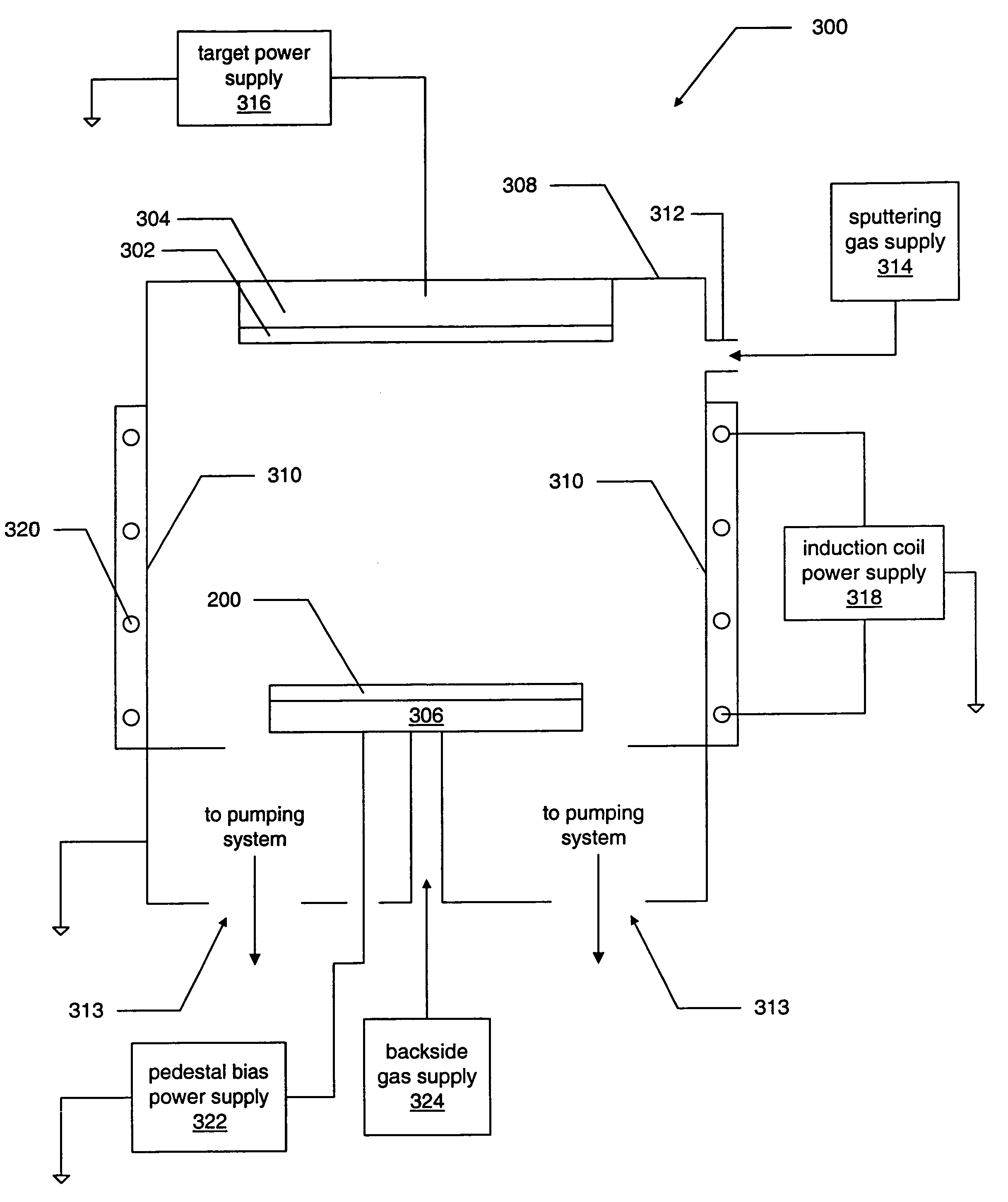
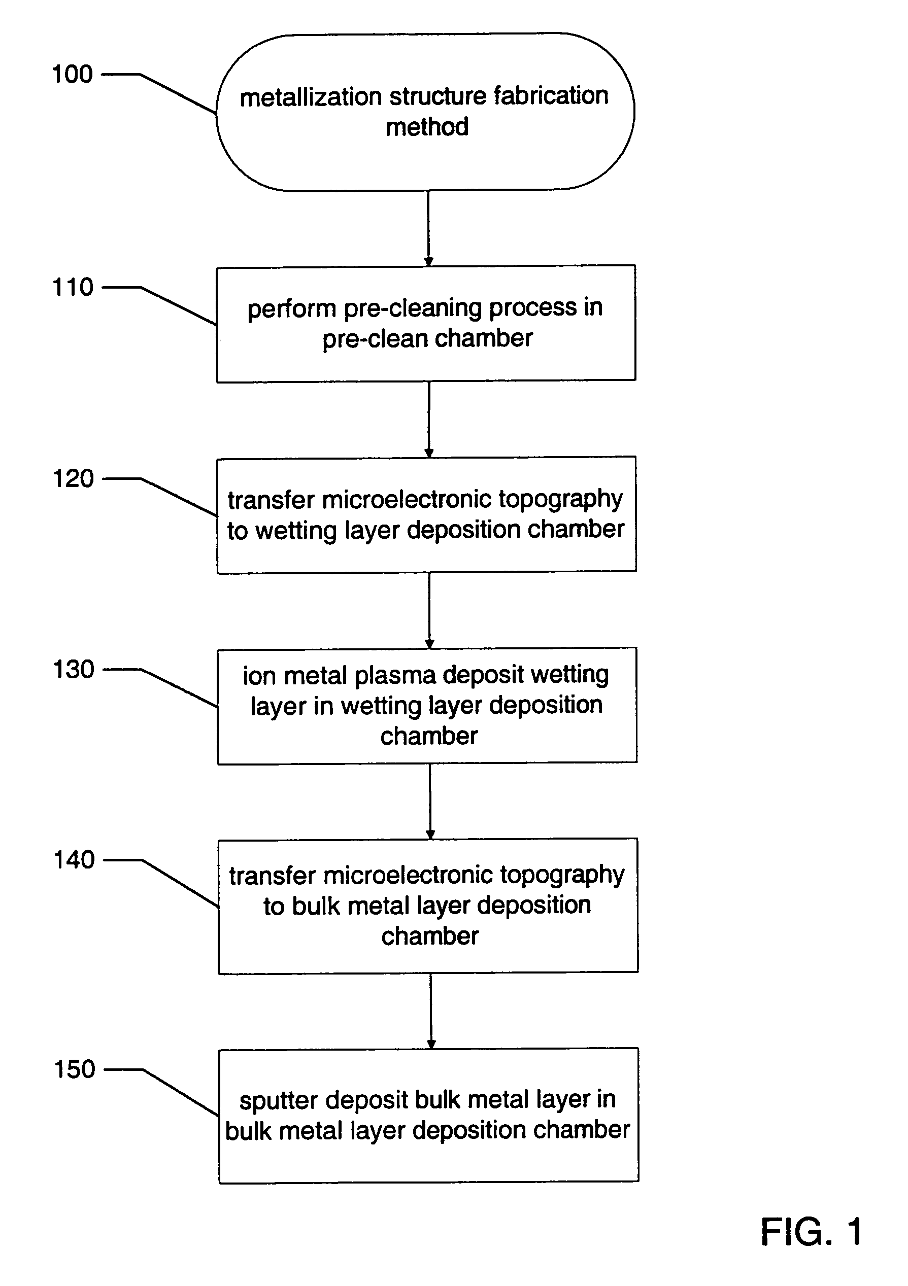
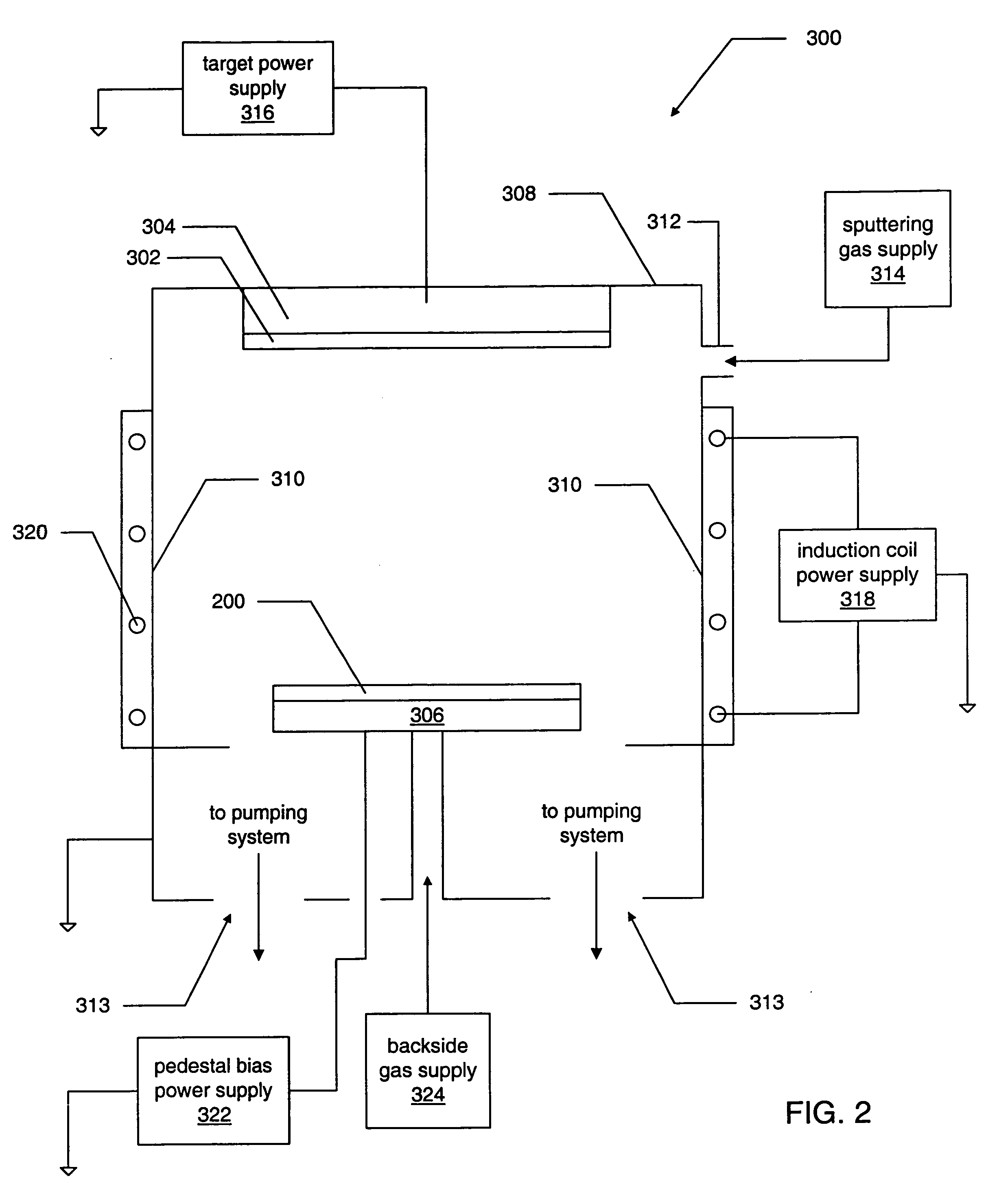
[0039]FIG. 1 presents a flow chart of a method for fabricating a metallization structure in accordance with a preferred embodiment. Metallization structure fabrication method 100 illustrates a preferred embodiment of the present method. While there may be any number of processing steps performed before and after the steps shown in method 100, method 100 preferably includes a preliminary step 110 of performing a pre-cleaning process.

[0040]In FIG. 4, however, a cross-sectional view of a microelectronic topography suitable for use in an embodiment is shown as configured before performing step 110. Microelectronic topography 200 is shown with a dielectric layer 202 arranged above a lower portion 201 of the microelectronic topography. Microelectronic topography lower portion 201 may include a substrate and any layers and materials formed above the substrate from which microelectronic products (e.g., semiconductor devices) may be produced. Preferably, microelectronic topography lower port...


PUM

PropertyMeasurementUnit
Fractionaaaaaaaaaa
Temperatureaaaaaaaaaa
Electrical conductoraaaaaaaaaa

Abstract

A method for fabricating a metallization structure is presented. The method preferably includes ion metal plasma depositing a wetting layer within a cavity defined in a dielectric layer. The wetting layer preferably includes titanium. The method preferably further includes sputter depositing a bulk metal layer within the cavity and upon the wetting layer. Sputter depositing of the bulk metal layer is preferably performed in a single deposition chamber at least until the cavity is substantially filled.

Description

BACKGROUND OF THE INVENTION[0001]1. Field of the Invention[0002]This invention relates to integrated circuit fabrication and, more particularly, to methods for forming metallization structures.[0003]2. Description of the Related Art[0004]The information described below is not admitted to be prior art by virtue of its inclusion in this Background section.[0005]An integrated circuit includes numerous active and passive devices arranged upon and within a single substrate. In order to implement desired circuit functions, select devices or components of the integrated circuit must be interconnected. Metallization structures are often used to interconnect integrated circuit components. Metallization structures may be generally subdivided into two categories: laterally extending interconnect lines and vertically extending contacts or plugs. Interconnects are relatively thin lines of conductive material that largely extend parallel to the underlying devices. As the name implies, contacts ar...

Claims


Application Information

Patent Timeline
IPC IPC(8): C23C14/04C23C14/34H01L21/285C23C14/35C23C14/54H01L21/28H01L21/3205H01L21/44H01L21/768H01L23/52
CPCC23C14/046C23C14/358C23C14/541H01L21/2855H01L21/76843H01L21/76865H01L21/76876H01L21/76877H01L21/76804H01L21/28
Inventor LAU, GORLEY L.
Owner MONTEREY RES LLC
Why Eureka
Try Eureka