Encapsulated organic electroluminescent display
- Summary
- Abstract
- Description
- Claims
- Application Information
AI Technical Summary
Benefits of technology
Problems solved by technology
Method used
Image
Examples
first embodiment
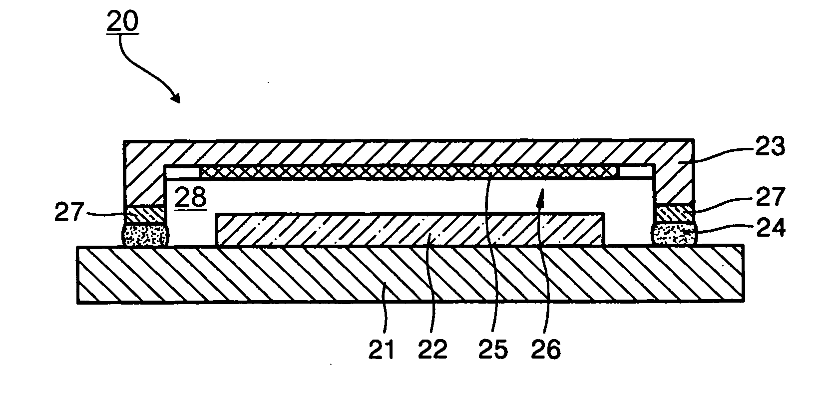
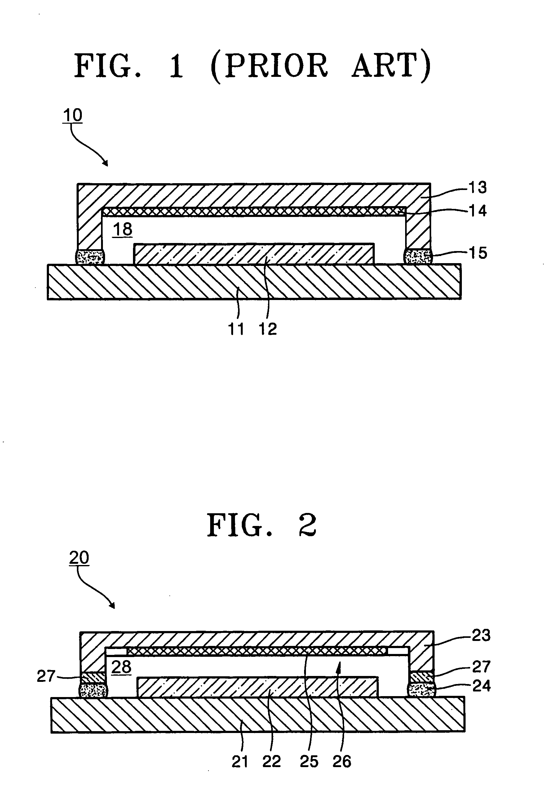
[0024] Turning now to FIG. 2, FIG. 2 illustrates an organic electroluminescent display 20 according to the present invention. Display 20 of FIG. 2 includes a substrate 21, an organic light-emitting unit 22 formed on a surface of the substrate 21, and an encapsulation cover 23 disposed above the organic light-emitting unit 22 and bonded to the substrate 21. The substrate 21 may be a glass substrate or a transparent insulating substrate.
[0025] The organic light-emitting unit 22 is encapsulated and sealed from the external elements by bonding the substrate 21 to the encapsulation cover 23. Organic light emitting unit 22 includes a first electrode attached to the substrate 21, a second electrode, and an organic layer that is a light-emitting layer sandwiched between the first and the second electrode. Alternatively, the organic light-emitting unit 22 can be a five-layered structure including a hole supplying layer and an electron supplying layer. The first electrode, the organic layer, ...
second embodiment
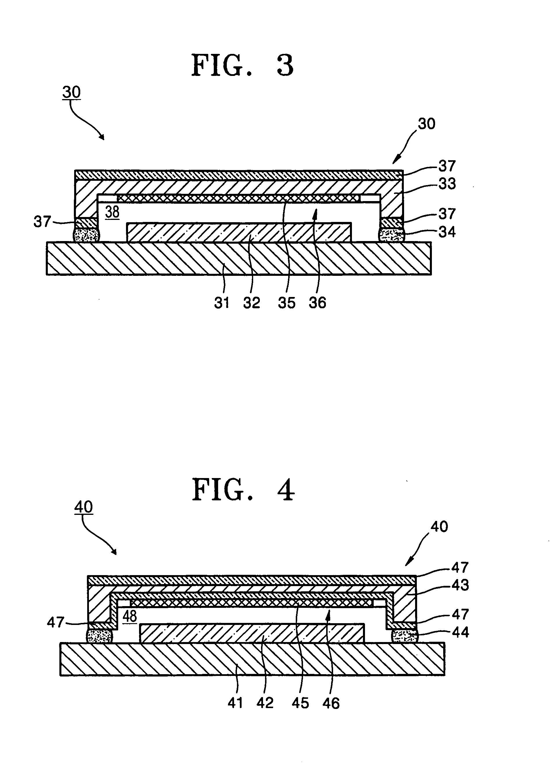
[0037] Referring to FIG. 3, a buffer layer 37 of an organic electroluminescent display 30 of the second embodiment is formed on the outer surface of the encapsulation cover 33, in addition to between the lower edge of the encapsulation cover 33 and the upper surface of the sealant 34. When encapsulation cover 33 bonded to a substrate 31, encapsulation cover 33 has a recess 36 formed on one side of the encapsulation cover 33. Absorbent layer 35 is on a bottom of recess 36 of encapsulation cover 33. After display 30 is completely formed, absorbent layer 35 faces an organic light-emitting unit 32 on substrate 31.
[0038] The encapsulation cover 33 provided with the buffer layer 37 and the recess 36 may be formed as follows. First, a glass that makes the encapsulation cover 33 is dip coated into a material that makes the buffer layer 37 to form the buffer layer 37 on both side of surfaces of the glass. Then, one side of the dip coated sodalime glass is etched, preferably via a completely ...
PUM
| Property | Measurement | Unit |
|---|---|---|
| Transparency | aaaaa | aaaaa |
Abstract
Description
Claims
Application Information
 - R&D
- Intellectual Property
- Life Sciences
- Materials
- Tech Scout
- Unparalleled Data Quality
- Higher Quality Content
- 60% Fewer Hallucinations
Browse by: Latest US Patents, China's latest patents, Technical Efficacy Thesaurus, Application Domain, Technology Topic, Popular Technical Reports.
© 2025 PatSnap. All rights reserved.Legal|Privacy policy|Modern Slavery Act Transparency Statement|Sitemap|About US| Contact US: help@patsnap.com


