Magnetically enhanced power inductor with self-aligned hard axis magnetic core produced using a damascene process sequence
- Summary
- Abstract
- Description
- Claims
- Application Information
AI Technical Summary
Benefits of technology
Problems solved by technology
Method used
Image
Examples
Embodiment Construction
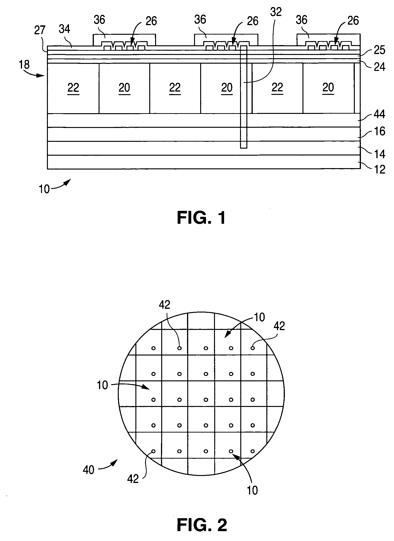
[0021]FIG. 1 shows a cross section of a semiconductor integrated circuit die 10 with power circuitry and an inductor fabricated directly thereon. The die 10 includes a silicon substrate 12 with the power circuitry fabricated thereon in accordance with well known semiconductor manufacturing techniques (for the sake of simplicity, the power circuitry is not shown in FIG. 1). The die 10 also has metal interconnect layer(s) 14, including one or more levels of metal interconnect, and an upper dielectric layer 16 (e.g., a die passivation layer) formed over the metal interconnect layers 14. An inductor structure 18 is fabricated directly on a plating layer 44 that is formed over the interconnect dielectric layer 16. The inductor 18 includes a plurality of magnetic core inductor members 20 provided between spacers 22, a planarization surface 24 formed over the inductor members 20 and spacers 22, an insulating layer 25, another plating layer 27, an inductor coil 26, a protective layer 34 for...
PUM
| Property | Measurement | Unit |
|---|---|---|
| Magnetic field | aaaaa | aaaaa |
| Electrical conductor | aaaaa | aaaaa |
| Height | aaaaa | aaaaa |
Abstract
Description
Claims
Application Information
 - R&D
- Intellectual Property
- Life Sciences
- Materials
- Tech Scout
- Unparalleled Data Quality
- Higher Quality Content
- 60% Fewer Hallucinations
Browse by: Latest US Patents, China's latest patents, Technical Efficacy Thesaurus, Application Domain, Technology Topic, Popular Technical Reports.
© 2025 PatSnap. All rights reserved.Legal|Privacy policy|Modern Slavery Act Transparency Statement|Sitemap|About US| Contact US: help@patsnap.com


