Method of polishing semiconductor wafer

Inactive Publication Date: 2005-11-29
SHIN-ETSU HANDOTAI CO LTD
View PDF9 Cites 1 Cited by
  • Summary
  • Abstract
  • Description
  • Claims
  • Application Information

AI Technical Summary

Benefits of technology

[0011]The present invention has been made in light of the above problem in the prior art and it is an object of the present invention to provide a method for polishing a semiconductor wafer, in which by using a specific polishing cloth as one for use in a mirror polishing step for a semiconductor wafer, especially in a final polishing stage thereof, there is prevented generation of micro-scratches and blind scratches on a wafer surface.
[0014]This is considered because by making longer the nap length, a wafer is polished while keeping elasticity of a surface layer of a final polishing cloth which is brought into direct contact with the wafer at a more proper level than before, or fine particles of impurities that can be a cause for scratches are captured perfectly within the longer nap layer; generation of the scratches is suppressed.
[0016]In the above polishing cloth of the three layers, as the hard plastic sheet, there can be used plastic classified in a category of a relatively hard type such as polyethylene terephthalate (PET), polyimide, polyethylene or polyurethane. Further, as the elastic sheet, there can be preferably used a sponge-like rubber elastic material such as foamed silicone rubber or foamed urethane rubber. When using such a polishing cloth, by making longer the nap length, with almost no generation of micro-scratches and blind scratches, there is suppressed propagation of waviness of the polishing cloth, especially waviness of the bottom layer section thereof, to the surface section caused by horizontal force during processing, and there is improved non-uniformity in an amount of stock removal caused by sori (bow or warp) and waviness of the wafer itself so as to upgrade an ability to maintain flatness on the whole wafer; there is obtained a mirror polished wafer in which a peripheral sag is prevented, and which is excellent in flatness and surface roughness.
[0017]As a polishing stage using the above polishing cloths, a final polishing stage is preferable. The term “final polishing” used in the present invention means polishing in the final stage of the polishing step including plural polishing stages. While polishing using a polishing cloth having a nap layer is considered to be applied to other than the final polishing stage, by applying the polishing method of the present invention to a final polishing stage, micro-scratches (polishing slight scratches) caused in the final polishing stage can be prevented.
[0018]The reason why a nap length of a polishing cloth used in the method of the present invention is set to be 500 μm or more is that it has been found that with a polishing cloth with such a nap length, signals (micro-scratches) of 0.10 μm or less greatly decreases in evaluation with a particle counter and it has also become clear that with a polishing cloth with a nap length of 500 μm or more, generation of micro-scratches caused by processing can be prevented. While the upper limit of the nap length is not specifically limited, it is hard to make a polishing cloth with an excessively long nap length; therefore, it is considered that the upper limit of the nap length is about 600 μm under the present circumstances.

Problems solved by technology

By generation of such scratches, there arises a problem that product yield decreases in a device fabrication process and other processes.
Further, a blind scratch on a wafer surface is a defect (damage) that cannot be observed in ordinary appearance inspection and evaluated with a method wherein a wafer is subjected to preferential etching, followed by observation.

Method used


Image

  • Method of polishing semiconductor wafer
  • Method of polishing semiconductor wafer
  • Method of polishing semiconductor wafer

Examples


examples 1 and 2

[0045]Using polishing cloths each with a structure similar to those of Comparative Examples 1 and 2, in which surface layer sections FS-3 of the suede type final polishing cloths were replaced by FS-7 (a trade name, made by Daiichi Lace K.K.) having a nap layer of 520 μm (Example 1) and FS-7 having a nap layer of 70 μm (Example 2), respectively, to form three layer structures of FS-7 / #188PET / HN-400, polishing was performed in the same conditions and with the same polishing agent as in Comparative Examples 1 and 2.

[0046]In Examples 1 and 2, polishing micro-scratches and blind scratches were hardly generated. Typical polishing results of a wafer (W) (results of Example 1) are shown in FIG. 6 (polishing micro-scratches) and FIG. 7 (blind scratches). Note that the count number of polishing micro-scratches (0.10 μm to 0.09 μm in particle diameter) in FIG. 6 was 74.

[0047]The results of Comparative Examples 1 and 2 (FS-3 / #188PET / HN-400) and the results of Examples 1 and 2 (FS-7 / #188PET / HN-...

examples 3 and 4

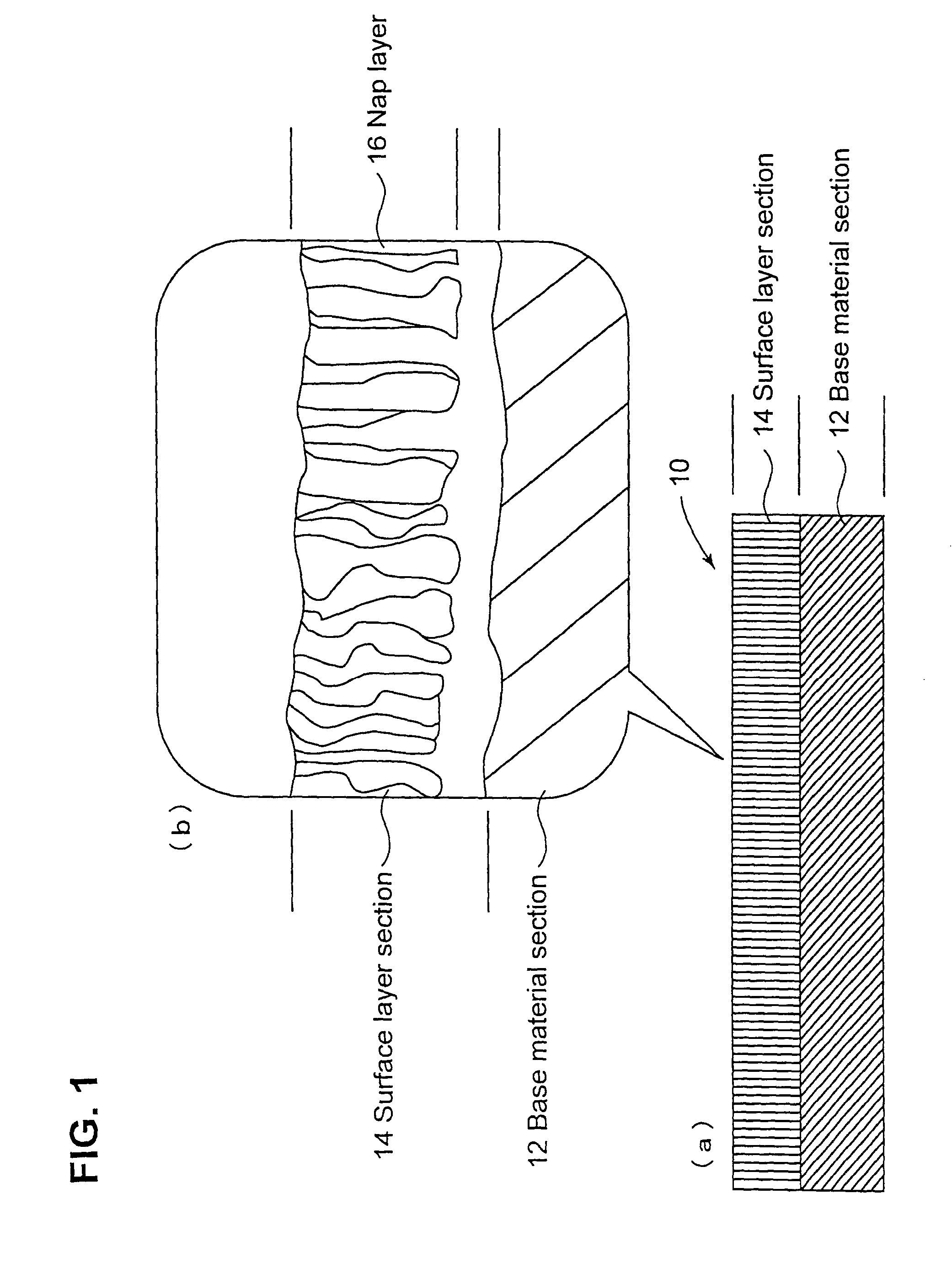
[0050]Using polishing cloths each of a structure similar to those of Comparative Examples 3 and 4 (the two layer polishing cloth of FIG. 1), in which nap layers were changed to one of 530 μm (Example 3) and another of 550 μm (Example 4), respectively, wafers were polished in a manner similar to Comparative Examples 3 and 4.

[0051]As a result, micro-scratches (polishing slight scratches) and blind scratches on a wafer surface were hardly observed when both the above polishing cloths were used.

example 5

[0052]A batch polishing apparatus similar to the apparatus used in Comparative Examples 3 and 4 was used and a polishing cloth of a three layer structure was adopted as a final polishing cloth.

[0053]As the three layer polishing cloth, FS-7 / #188PET / HN-400 having a nap layer of 570 μm (similar to Example 2) was used.

[0054]As a result, micro-scratches and blind scratches on a wafer surface were not observed. Further, flatness in a peripheral portion of each wafer was better than when the two layer polishing cloth was used.

[0055]As described above, it has been found that there can be prevented generation of polishing micro-scratches (slight scratches) and blind scratches on a wafer surface depending on a length of a nap layer, regardless of types of polishing apparatus (a batch type or a single wafer type), and independently of types of polishing cloths such as a two layer one or a three layer one. Especially, it is effective to use a final polishing cloth with a nap length of 500 μm or...


PUM

PropertyMeasurementUnit
Thicknessaaaaaaaaaa
Thicknessaaaaaaaaaa

Abstract

There is provided a method for polishing a semiconductor wafer, in which by using a specific polishing cloth as one for use in a mirror polishing step for the semiconductor wafer, especially in a final polishing stage thereof, generation of micro-scratches and blind scratches on a wafer surface is prevented. In a polishing step of mirror polishing the semiconductor wafer using a polishing cloth, the polishing is performed using the polishing cloth with a nap layer of 500 μm or more in thickness.

Description

TECHNICAL FIELD[0001]The present invention relates to a method for polishing a semiconductor wafer (hereinafter also simply referred to as a wafer), in which by using a specific polishing cloth as one for use in a mirror polishing step for the semiconductor wafer, especially in a final polishing stage thereof, there is prevented generation of micro-scratches and blind scratches on a wafer surface.BACKGROUND ART[0002]A manufacturing process for a semiconductor wafer includes the following steps: a slicing step of slicing thin plates (wafers) from a single crystal ingot, and other steps such as chamfering a wafer, lapping, etching, polishing, and cleaning.[0003]A chemical etched wafer surface is processed in a mirror polishing into a mirror-surface having smoothness without strain. Mirror polishing of a silicon wafer is conducted while giving a prescribed load and a relative speed between the wafer and the polishing cloth, and supplying a polishing agent. As the polishing agent there ...

Claims


Application Information

Patent Timeline
IPC IPC(8): B24B37/20B24B37/22B24B37/24B24D13/12B24D13/14H01L21/304H01L21/306
CPCB24B37/22B24B37/24H01L21/02024H01L21/304
Inventor TAKANASHI, KAZUHITOSUZUKI, KIYOSHIWATANABE, YOSHINORI
Owner SHIN-ETSU HANDOTAI CO LTD
Why Eureka
Try Eureka