Three-dimensional nonwoven substrate for circuit board

a nonwoven substrate and circuit board technology, applied in the direction of printed circuit stress/warp reduction, conductive pattern formation, circuit electrical arrangement, etc., can solve the problems of difficult handling, high cost, and high cost of weaving fiberglass, so as to improve structural performance, prevent cracking, and unique and useful performance properties

Inactive Publication Date: 2005-11-15
POLYMER GROUP INC
View PDF28 Cites 3 Cited by
  • Summary
  • Abstract
  • Description
  • Claims
  • Application Information

AI Technical Summary

Benefits of technology

[0008]By the utilization of a hydroentangled, three-dimensionally imaged support substrate impregnated with a durable resinous matrix, PCB's, and similar applications, can be imparted with unique and useful performance properties, to improve structural performance. The substrate can be directly imparted with inherent properties, which have heretofore required the manufacture of multiple components and fabrication into a useful article, such as: “Reinforcements”, to counteract temporary (flex) and permanent (warp) strains, “bolsters”, around through-holes at mounting points to prevent cracking, and “guides”, for mounting other pieces to the base construct. As well as articles such as, “registration markers”, to aid in establishing proper reference orientation during fabrication procedures and automated quality control analyses, “live hinges”, which focus flexural energy into a region of the substrate which is most able to accommodate such energy, “rail stops”, to prevent exceeding an established reference point during the fabrication of the individual construct or when such constructs are combined into a more complex matrix, “cavities”, to allow for the formation of recesses in which to place bulky or otherwise hindered pieces, “apertures”, to create a pre-existing through-hole without the need of drilling, “drilling targets”, a version based on having an aperture will with only resinous binder. Common and predictable fibrous composition of the matrix in the target facilitates the ability to automate drill-out process, whether in consistency of wattage required to ablate by way of laser, or in drill-bit performance over a finite time period.
[0009]To improve the thermal performance of the circuit board, the hydroentangled, three-dimensionally imaged nonwoven support substrate can be constructed such that the presence of heat, which generally has a deleterious effect on electronic components, can be controlled or directed. For instance, the conduction of thermal energy can be directed from a first specified region to a second specified region. Mass sinking can be controlled, whereby a region of increased mass can be utilized as an endpoint for a thermal conduction path. Further, dynamic sinking can be controlled, whereby a region having the ability to be actively cooled can be utilized as an endpoint for a thermal conduction path. Further still, the nonwoven substrate can be formed into useful cooling projections, such as posts or fins, which combines dynamic sinking with a structural capability.
[0010]It is also in the purview of the present invention that the substrate improves the electrical performance of the circuit board. The substrate can be constructed such that when employed as a base for electrical circuitry, certain and specific regions of the substrate exhibit performance beneficial or directly employed by the electronic components attached thereto or thereupon. A specific example of performance-orientated regions include those, which have variable, specific, and / or isolated dielectric attributes. The variable dielectric region may be of a corresponding variance in bulk, or of uniform bulk and the variance a property of mass. The nonwoven support substrate can be used for grounding purposes so as to impart a PCB with the ability to control the buildup of static charge and / or the ability to protect sensitive electronic components from overcharge, as well as provide a PCB with electromagnetic shielding by dissipating an electrical charge induced by a magnetic field.
[0012]It is also within the purview of the invention that the substrate may be comprised of a single layer construct or a multi-layer construct. The layers can either be woven substrates, nonwoven substrates, or the combination thereof and may be of the same or differing composition. Further, the support substrate may be of a laminate or composite structure. Further still, the substrate can be integrated, wherein formation of the substrate includes alternate materials to impart different physical properties (i.e. incorporation of a carbon fiber into a PET nonwoven or a glass woven to create an electro conductive substrate). Additionally, the substrate can include alternate materials to enhance physical properties (i.e. use of oriented monofilament or variable denier to reduce elongation). Use of flame-retardant or self-extinguishing component in substrate allow for protection of sensitive circuitry in case of catastrophic thermal failure.

Problems solved by technology

The production of conventional textile substrates for PCB and like applications is known to be a complex, multi-step process.
Weaving fiberglass is known to be highly detrimental to weaving components, as well as difficult to handle due to hazards imposed by the fine glass filaments.

Method used


Image

  • Three-dimensional nonwoven substrate for circuit board
  • Three-dimensional nonwoven substrate for circuit board
  • Three-dimensional nonwoven substrate for circuit board

Examples


Embodiment Construction

[0018]While the present invention is susceptible of embodiment in various forms, there is shown in the drawings and will hereinafter be described a presently preferred embodiment of the invention, with the understanding that the present disclosure is to be considered as an exemplification of the invention, and is not intended to limit the invention to the specific embodiment illustrated.

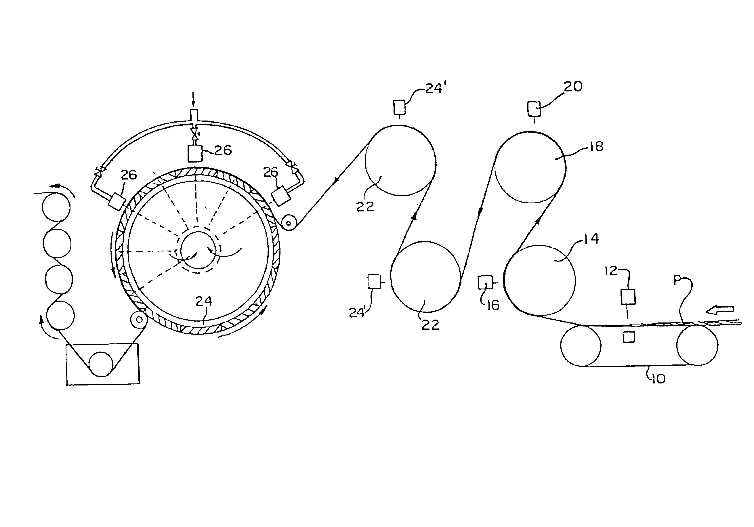
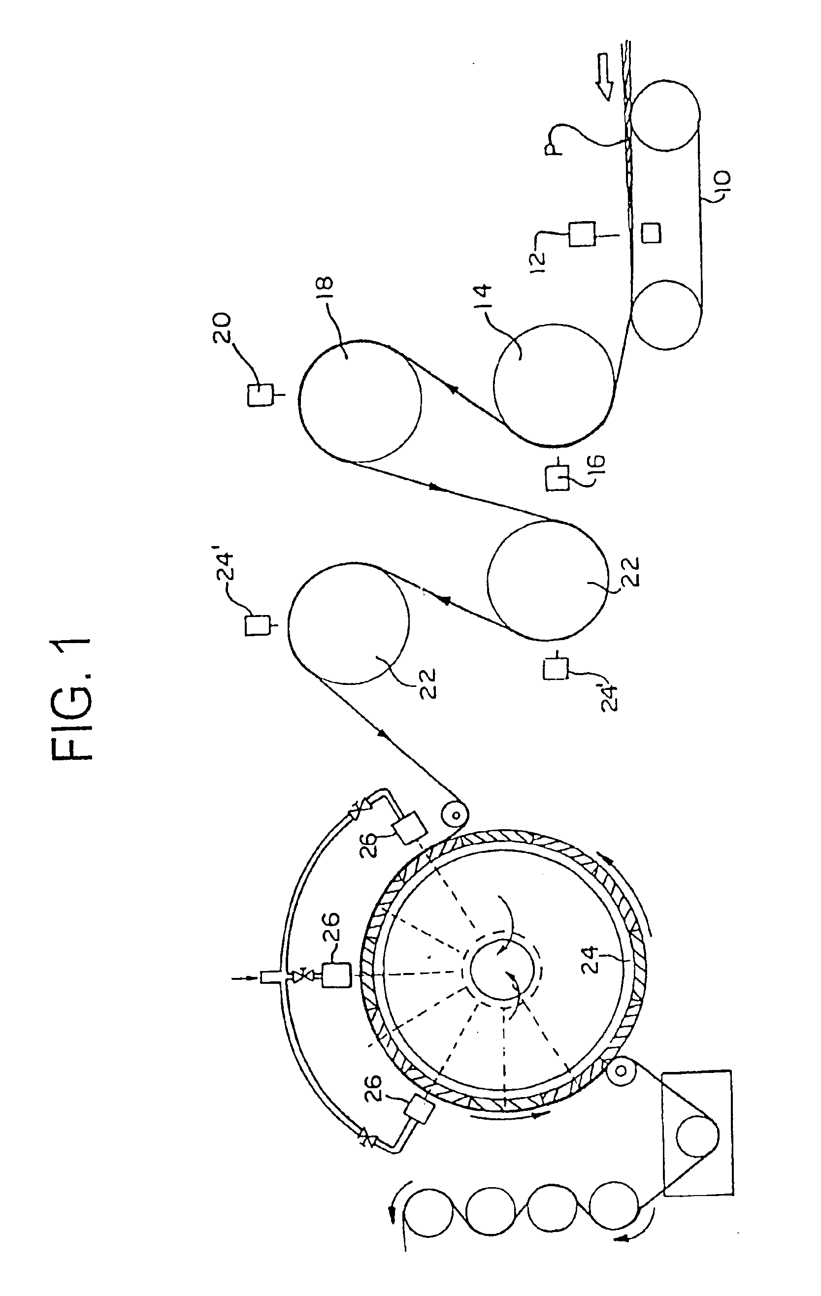
[0019]Manufacture of a three-dimensionally imaged nonwoven substrate embodying the principles of the present invention is initiated by providing the fibrous matrix, which can include the use of staple length fibers, continuous filaments, and the blends of fibers and / or filaments having the same or different composition. Fibers and / or filaments are selected from natural or synthetic composition, of homogeneous or mixed fiber length. Suitable natural fibers include, but are not limited to, cotton, wood pulp and viscose rayon, flax, hemp, and kenaf. Natural fibers also include silicates, such as glass. ...


PUM

PropertyMeasurementUnit
lengthsaaaaaaaaaa
lengthsaaaaaaaaaa
resinousaaaaaaaaaa

Abstract

The present invention relates to a nonwoven substrate, and specifically to a nonwoven substrate imparted with a three-dimensional image, wherein the three-dimensional nonwoven substrate is particularly suited as a support substrate for a PCB (Printed Circuit Board) and similar application.By the utilization of a hydroentangled, three-dimensionally imaged support substrate impregnated with a durable resinous matrix, PCB's, and similar applications, can be imparted with unique and useful performance properties, to improve structural performance.

Description

TECHNICAL FIELD[0001]The present invention relates generally to a nonwoven substrate, and specifically to a nonwoven substrate imparted with a three-dimensional image, wherein the three-dimensional nonwoven substrate is particularly suited as a support substrate for a PCB (Printed Circuit Board) and similar applications.BACKGROUND OF THE INVENTION[0002]The production of conventional textile substrates for PCB and like applications is known to be a complex, multi-step process. The production of such substrates from staple fibers begins with the carding process where the fibers are opened and aligned into a feedstock known as sliver. Several strands of sliver are then drawn multiple times on a drawing frames to further align the fibers, blend, improve uniformity as well as reduce the sliver's diameter. The drawn sliver is then fed into a roving frame to produce roving by further reducing its diameter as well as imparting a slight false twist. The roving is then fed into the spinning f...

Claims


Application Information

Patent Timeline
Patent Type & Authority Patents(United States)
IPC IPC(8): B29B15/10B29B15/12B29C70/12B29C70/10B29C70/16D04H1/46H05K1/03C08J5/04B29C70/36B29C70/50B32B5/24D04H1/48D04H3/10D04H5/02D04H13/00H05K1/00H05K1/02H05K3/00H05K3/10
CPCB29B15/122B29C70/12B29C70/16B29C70/50D04H1/465D04H1/48D04H3/102D04H5/02H05K1/0271H05K1/0366B29L2031/3425H05K1/0254H05K1/0272H05K1/0393H05K3/0052H05K3/107H05K2201/0129H05K2201/0278H05K2201/0284H05K2201/0293H05K2201/09045H05K2201/09127H05K2201/2009H05K2201/2036H05K2203/065D04H1/49D04H1/495D04H3/11D04H5/03Y10T442/259Y10T442/689
Inventor ZUCKER, JERRYCARTER, NICK MARK
Owner POLYMER GROUP INC
Why Eureka
Try Eureka