Leakage compensation circuit
a compensation circuit and dielectric technology, applied in the field of electronic circuits, can solve the problems of reducing performance, affecting the operation of the oscillator, and causing significant dielectric leakage,
- Summary
- Abstract
- Description
- Claims
- Application Information
AI Technical Summary
Benefits of technology
Problems solved by technology
Method used
Image
Examples
first embodiment
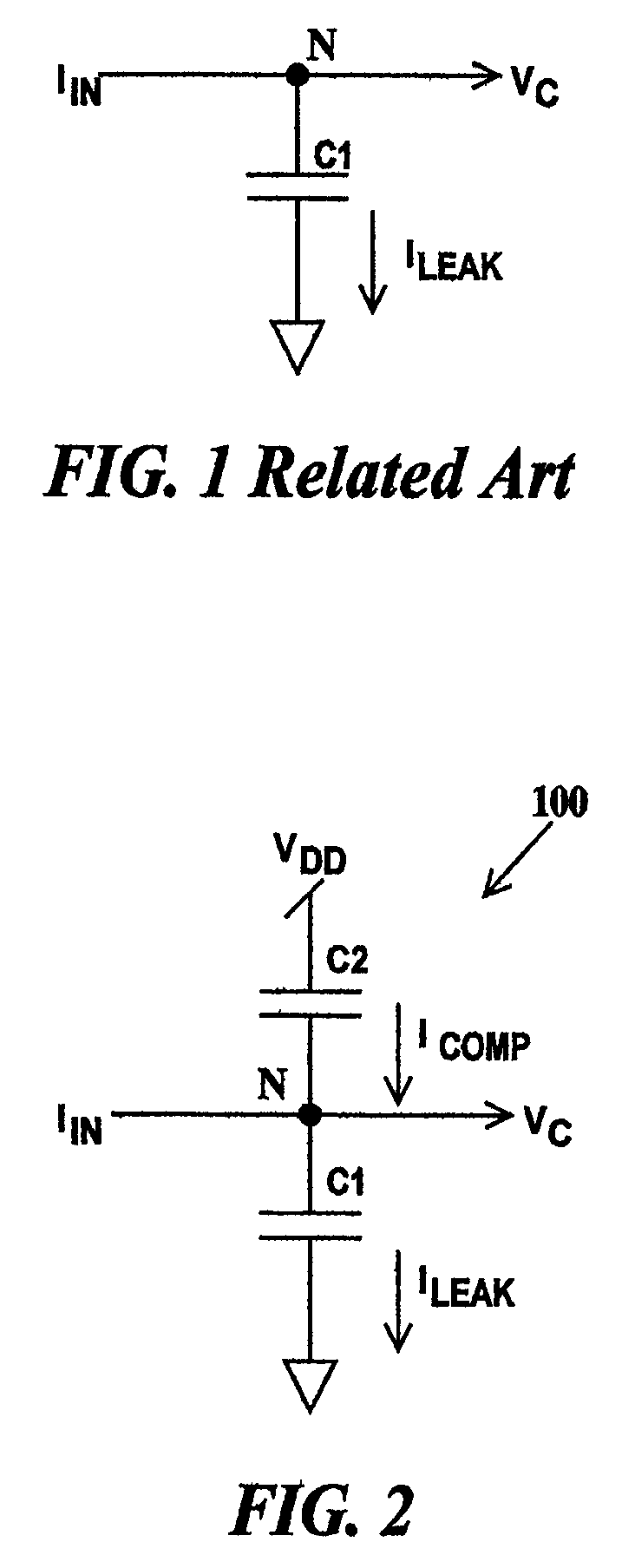
[0023]FIG. 2 is a schematic diagram of a circuit 100 illustrating a method for compensating for leakage through a capacitor according to the present invention. In FIG. 2, input currentIN is applied to node N and output voltage VC is supplied from node N. Capacitor C1 is connected between node N and ground. Node N is coupled to a voltage source VDD through capacitor C2. Current IIN charges capacitor C1 maintaining voltage VC at a predetermined level that varies as IIN varies. However, if capacitor C1 is leaky a leakage current ILEAK will flow to ground causing voltage VC to drop from its predetermined value between refresh cycles of IIN. A compensation capacitor C2 is connected between node N and voltage source VDD. Compensation capacitor C2 is charged by voltage source VDD and leaks a compensation current ICOMP. When current ICOMP is equal to current ILEAK voltage VC will remain constant between current IIN refresh cycles. Current ICOMP is equal to current ILEAK when (1) the capacit...
second embodiment
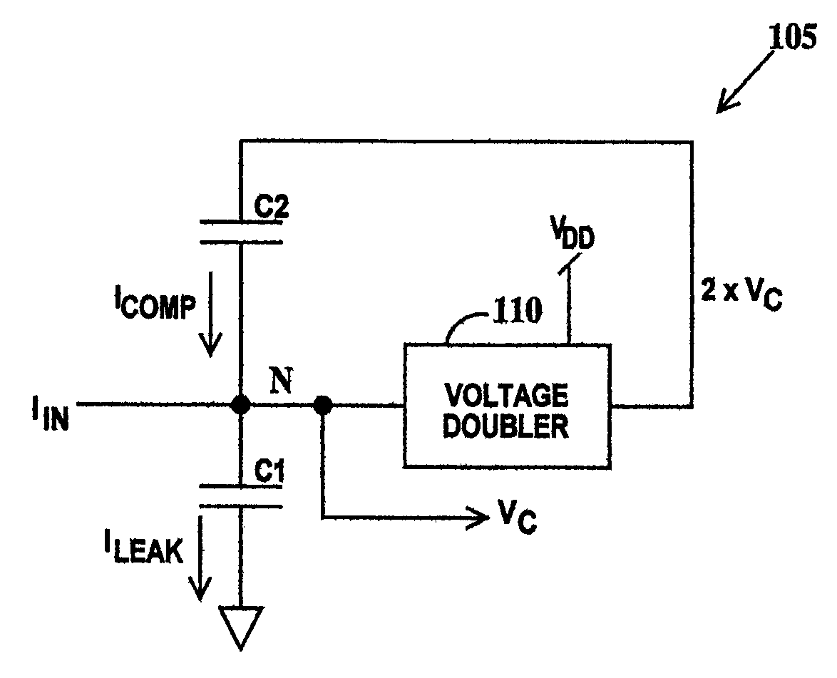
[0026]FIG. 3 is a block diagram of a circuit 105 illustrating a method for compensating for leakage through a capacitor according to the present invention. In FIG. 3, input currentIN is applied to node N and output voltage VC is supplied from node N. Capacitor C1 is connected between node N and ground. A first plate of a compensation capacitor C2 is connected to node N and a second plate of capacitor C2 is connected to the output of a voltage doubler 105. The input of voltage doubler 105 is connected to node N. Voltage doubler 105 thus generates an output voltage equal to twice voltage VC. Voltage doubler 105 is supplied by voltage source VDD. Capacitor C2 is charged by voltage doubler 110. Since leakage current is a function of capacitance and voltage across the capacitor, ICOMP will equal ILEAK when the capacitance of capacitor C1 and C2 are equal and the voltage across capacitors C1 and C2 is the same. Therefore voltage VC will remain constant between current IIN refresh cycles w...
third embodiment
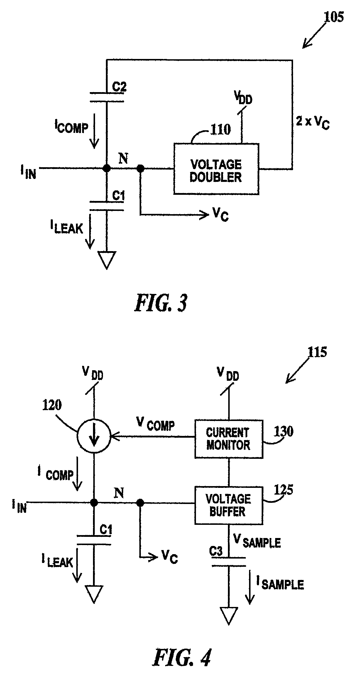
[0029]FIG. 4 is a block diagram of a circuit 115 illustrating a method for compensating for leakage through a capacitor according to the present invention. In FIG. 4, input current IIN is applied to node N and output voltage VC is supplied from node N. Capacitor C1 is connected between node N and ground. Compensation current ICOMP is supplied to node N by a variable current source 120 connected to voltage source VDD. A voltage buffer 125 is connected between node N and a current monitor 130. A current monitor 130 is connected between the control input of current source 120 and voltage buffer 125. Current monitor 130 is connected to voltage source VDD. A sampling capacitor C3 is connected between voltage buffer 125 and ground. Voltage buffer 125 generates a sample voltage VSAMPLE that is equal to voltage VC. (A voltage buffer transfers voltage at its input to voltage at its output without adding current load.) Voltage VSAMPLE charges capacitor C3 and capacitor C3 leaks a leakage curr...
PUM
 Abstract
Description
Claims
Application Information
 - R&D
- Intellectual Property
- Life Sciences
- Materials
- Tech Scout
- Unparalleled Data Quality
- Higher Quality Content
- 60% Fewer Hallucinations
Browse by: Latest US Patents, China's latest patents, Technical Efficacy Thesaurus, Application Domain, Technology Topic, Popular Technical Reports.
© 2025 PatSnap. All rights reserved.Legal|Privacy policy|Modern Slavery Act Transparency Statement|Sitemap|About US| Contact US: help@patsnap.com


