High frequency power amplifier

a power amplifier and high frequency technology, applied in the field of high frequency communication, can solve the problems of reducing the price of those amplifiers, affecting and b>100/b>power consumption, etc., and achieve the effect of maximizing the output range of amplifiers

Inactive Publication Date: 2005-09-06
MICREL
View PDF6 Cites 8 Cited by
  • Summary
  • Abstract
  • Description
  • Claims
  • Application Information

AI Technical Summary

Benefits of technology

[0012]The bias circuit provides a DC bias voltage to the input of the inverter that forces the output of the inverter to be centered on a desired DC operating voltage. By selecting the DC bias voltage to be between the upper and lower supply voltages, the inverter can be forced to operate in its linear region. An AC (alternating current) signal at the input of the inverter will then be amplified by the inverter without distortion (clipping), so long as the amplitude of the AC signal is not large enough to drive the inverter out of its linear region.
[0014]This DC control provided by the op-amp ensures that the inverter will operate in its linear region as long as the input signal is not large enough to push either of the transistors of the inverter into saturation. Therefore, by setting the reference voltage midway between the upper and lower supply voltages, the output range of the amplifier can be maximized.

Problems solved by technology

However, as high-frequency amplifiers become more common in consumer goods (e.g., a radio-frequency (RF) amplifier in a cellular telephone), reducing the price of those amplifiers becomes increasingly important.
However, because current is always flowing through the voltage divider formed by resistors R_UP and R_DN, amplifier 100 can exhibit excessive power consumption.
This power inefficiency is generally undesirable, and can be particularly problematic in devices that run off of a self-contained power supply (a battery).
For example, using amplifier 100 in a cellular telephone to reduce the overall cost of the phone may result in an unacceptable decrease in talk time for that phone.

Method used


Image

  • High frequency power amplifier
  • High frequency power amplifier
  • High frequency power amplifier

Examples


Embodiment Construction

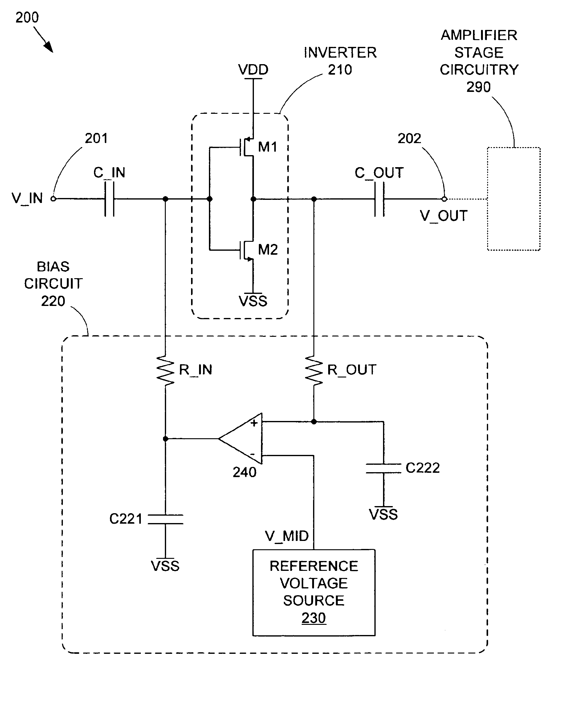
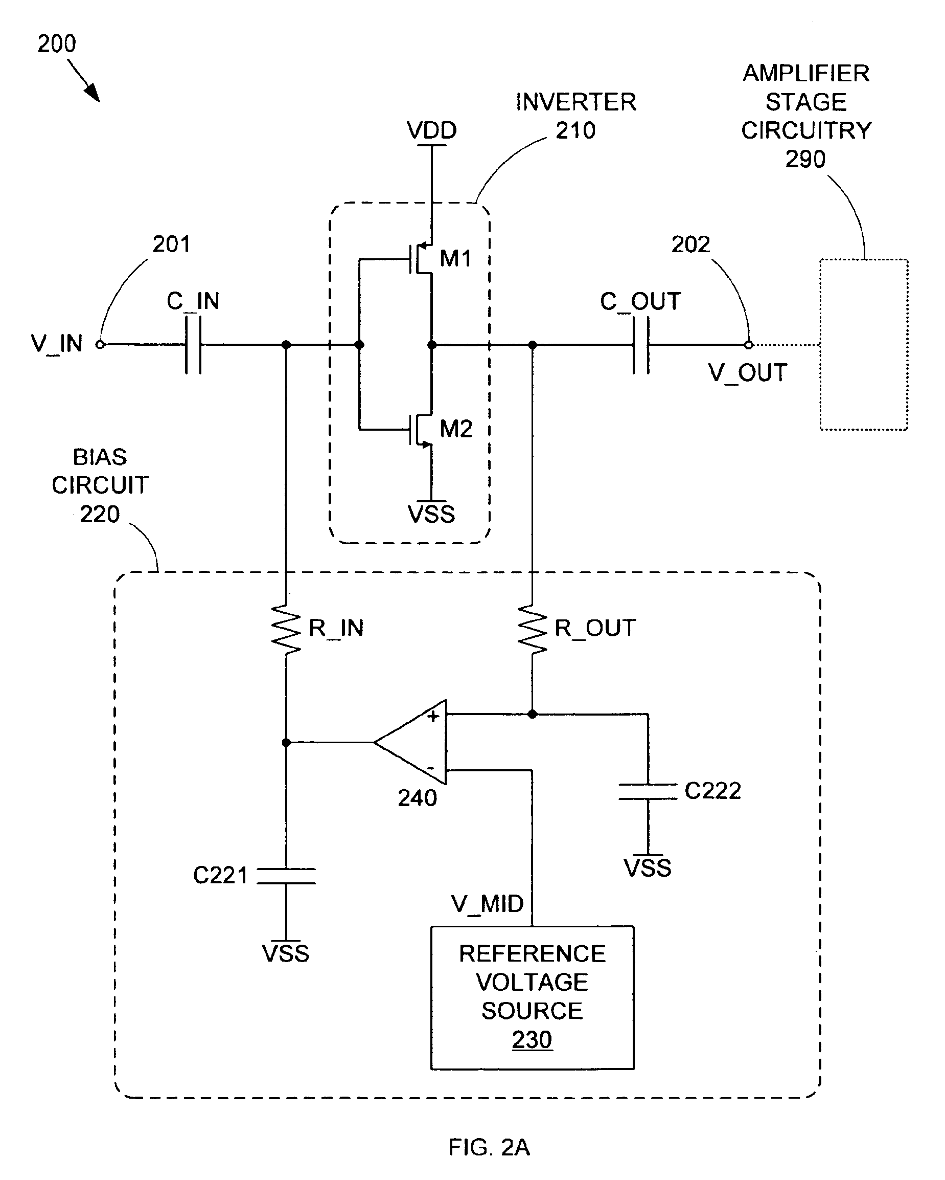
[0020]FIG. 2A shows a high-frequency amplifier circuit 200 in accordance with an embodiment of the invention. Amplifier circuit 200 includes an input terminal 201, an output terminal 202, a CMOS inverter 210, a capacitor C_IN, a capacitor C_OUT, and a bias circuit220. Capacitor C_IN is coupled between input terminal 201 and the input of inverter 210, while capacitor C_OUT is coupled between the output of inverter 210 and output terminal 202. Bias circuit 220 is connected between the output and input of inverter 210.

[0021]Inverter 210 includes a PMOS transistor M1 and an NMOS transistor M2 that are serially coupled between an upper supply voltage VDD and a lower supply voltage VSS (e.g., ground). The gate terminals of transistors M1 and M2 are connected to form the input of inverter 210, while the drain terminals of transistors M1 and M2 are connected to form the output of inverter 210.

[0022]Amplifier circuit 200 is coupled to receive an input high-frequency signal V_IN at input term...


PUM


Abstract

A CMOS amplifier includes a CMOS inverter and a bias circuit coupled in a feedback loop between the output and input of the inverter. The bias circuit provides linear biasing so that the inverter can apply a desired gain to a high frequency input signal. The bias circuit can include an operational amplifier (op-amp) providing positive feedback control between the output and input of the inverter. By providing a reference voltage to the other input of the op-amp, the input of the inverter is regulated such that its output is driven to the reference voltage. This in turn forces the inverter to operate in its linear region, so that the inverter applies non-distorting amplification to the input AC signal. The AC signal is prevented from affecting the operation of the bias circuit by resistors coupling the bias circuit to the op-amp.

Description

BACKGROUND[0001]1. Field of the Invention[0002]The invention relates to the field of high frequency communications, an in particular to a complementary metal-oxide-semiconductor high frequency amplifier.[0003]2. Related Art[0004]In a conventional high-frequency amplifier, a bipolar transistor (or transistors) is used to provide the desired signal gain, while also providing the responsiveness required to maintain signal integrity. However, as high-frequency amplifiers become more common in consumer goods (e.g., a radio-frequency (RF) amplifier in a cellular telephone), reducing the price of those amplifiers becomes increasingly important. One way to reduce costs is to implement the amplifier using a metal-oxide-semiconductor (MOS) or complementary MOS (CMOS) process instead of the more expensive bipolar process.[0005]FIG. 1 shows a conventional MOS RF amplifier 100. MOS amplifier 100 includes an input terminal 101, an output terminal 102, capacitors C1 and C2, resistors R_UP, R_DN, a...

Claims


Application Information

Patent Timeline
Patent Type & Authority Patents(United States)
IPC IPC(8): H03F3/18
CPCH03F1/0261H03F1/342H03F3/19H03F3/3022H03F2200/451H03F2200/555
Inventor MORAVEJI, FARHOOD
Owner MICREL
Why Eureka
Try Eureka