Method of producing a PTC-resistor device
a resistor and material technology, applied in the direction of overvoltage protection resistors, positive temperature coefficient thermistors, manufacturing tools, etc., can solve the problems of substantial energy dissipation of ptc-materials, and achieve the effect of improving the contact resistance between metal contact elements and ptc-polymer materials, improving current carrying capability, and efficient cooling of the web
- Summary
- Abstract
- Description
- Claims
- Application Information
AI Technical Summary
Benefits of technology
Problems solved by technology
Method used
Image


Examples
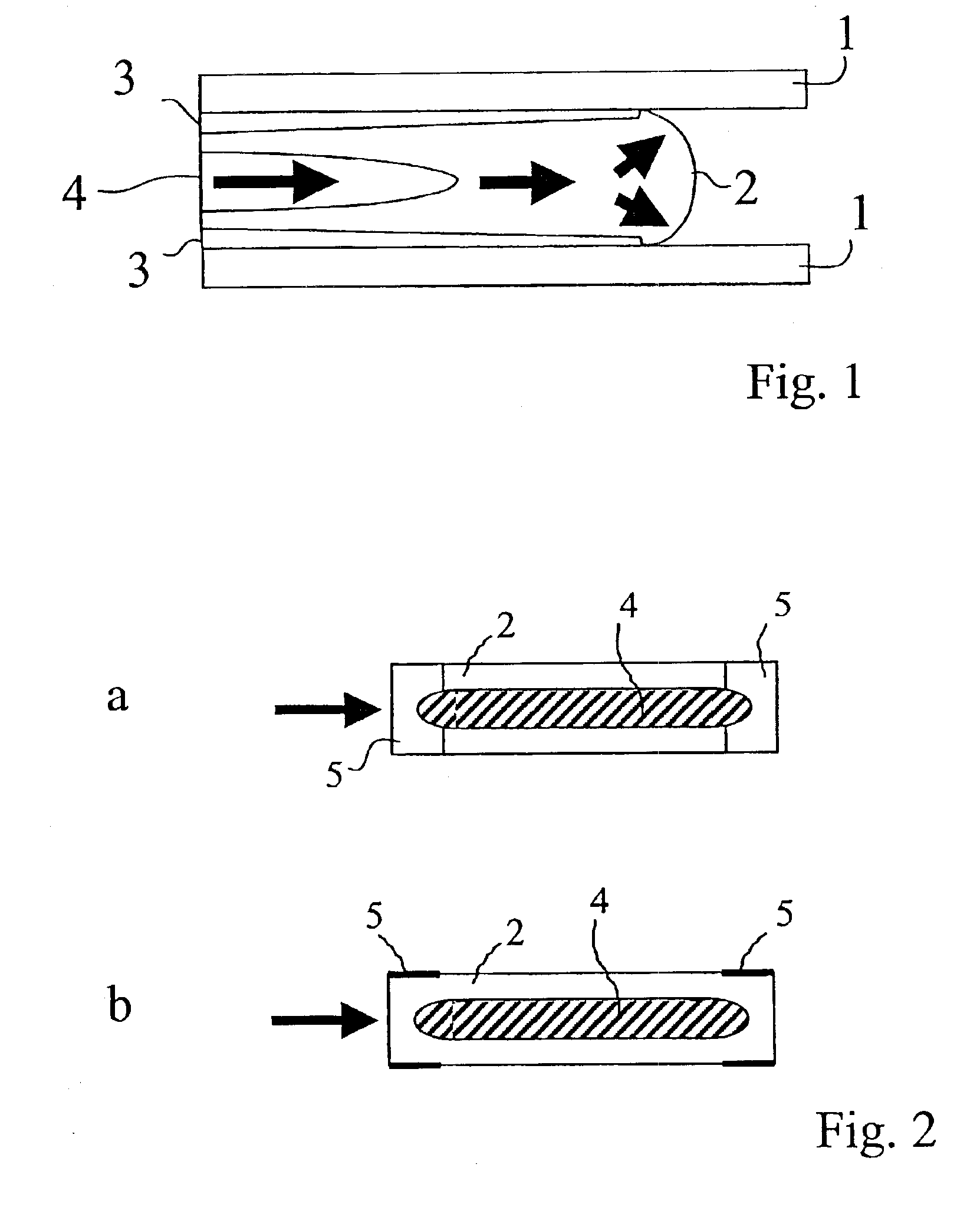
first embodiment
[0029]FIG. 2a is a schematic cross-sectional view of a resistor device according to the invention;
[0030]FIG. 2b is a view as in FIG. 2a but in different perspective;
second embodiment
[0031]FIG. 3a is a schematic cross-sectional view of a resistor device according to the invention;
[0032]FIG. 3b is a view as in FIG. 3a but in different perspective;
third embodiment
[0033]FIG. 4 is a schematic cross-sectional view of a resistor device according to the invention.
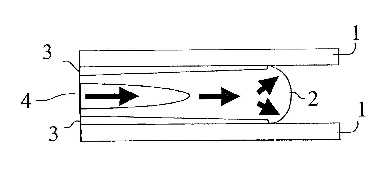
[0034]FIG. 1 is a diagram explaining the main principle of the invention. An injection mould is referenced by numeral 1 and symbolized by two cavity walls. It is clear that actual moulds can have much more complicated forms. The details of injection moulding technology need not be explained here and are known to the skilled person.
[0035]From a left side in FIG. 1, polymer material is introduced, as shown by the arrow, FIG. 1 shows a state in which a first material, a PTC-polymer material 2 had been injected earlier and has built-up a somewhat hardened peripheral layer near the walls of mould 1. This peripheral layer is referenced by numeral 3. Those parts of PTC-polymer material 2 that are not yet solidified and still fluid are followed by an (according to FIG. 1 presently) injected second material, a varistor polymer material 4. This varistor polymer material 4 pushes the fluid part of ...
PUM
| Property | Measurement | Unit |
|---|---|---|
| aperture angle | aaaaa | aaaaa |
| aperture angle | aaaaa | aaaaa |
| ) angle | aaaaa | aaaaa |
Abstract
Description
Claims
Application Information
 - R&D
- Intellectual Property
- Life Sciences
- Materials
- Tech Scout
- Unparalleled Data Quality
- Higher Quality Content
- 60% Fewer Hallucinations
Browse by: Latest US Patents, China's latest patents, Technical Efficacy Thesaurus, Application Domain, Technology Topic, Popular Technical Reports.
© 2025 PatSnap. All rights reserved.Legal|Privacy policy|Modern Slavery Act Transparency Statement|Sitemap|About US| Contact US: help@patsnap.com