
Method for preparing single crystal oxide thin film

a thin film and single crystal technology, applied in the direction of polycrystalline material growth, superconductor devices, condensed vapors, etc., can solve the problems of inability to achieve desired film quality, inability to maintain optimal thermodynamic equilibrium at the boundary of liquid and gas phases, and difficulty in conventional oxide thin film fabrication methods to provide. , to achieve the effect of excellent crystallinity and low melting poin

Inactive Publication Date: 2005-08-16
JAPAN SCI & TECH CORP
View PDF3 Cites 4 Cited by
  • Summary
  • Abstract
  • Description
  • Claims
  • Application Information

AI Technical Summary

Benefits of technology

The present invention provides a method for preparing a high-quality single crystal oxide thin film using a tri-phase epitaxy method. This method involves depositing a first oxide layer on a substrate, heating the substrate to melt a second layer, and depositing an oxide on the seed layer through a liquid layer formed by the melted second layer. By increasing the oxygen partial pressure on the liquid layer and optimizing process parameters, the method can achieve a desired film quality with large grain size. The resulting thin film has excellent properties and can be used for Josephson junction elements and other applications.

Problems solved by technology

However, it has been difficult for the conventional oxide thin-film fabrication methods to provide a desirable single crystal thin film without any crystal defect because of their principle of crystallizing the thin film directly from gas phase, and the crystallization reaction caused under a significantly non-thermodynamical equilibrium condition.
While the aforementioned TPE method as a new epitaxial thin-film growing method reported by the inventors provides a single crystal oxide thin film having a film quality equal to or slightly higher than that in the conventional PLD method, it has not been able to maintain optimal thermodynamical equilibrium at the boundary of the liquid and gas phases, and consequently a desired film quality has not been obtained.

Method used


Image

  • Method for preparing single crystal oxide thin film
  • Method for preparing single crystal oxide thin film
  • Method for preparing single crystal oxide thin film

Examples


example

Example 1

[0050]One example will be described in which an NdBa2Cu3O7 superconducting thin film was prepared using a conventional pulsed laser deposition apparatus in accordance with the method of the present invention. SrTiO3 (100) was used as a substrate. A sintered polycrystalline having the same composition and structure as a superconducting oxide to be formed was used as a target for depositing a seed layer and a film layer. This sintered polycrystalline was obtained by mixing RE2O3 powder, BaF2 or MaCO3 powder and CuO powder in conformity with the composition of the film layer, and heating the mixed powder at 1000° C. or more in a conventional electric furnace.

[0051]A mixed powder sintered body having the ratio of Ba:Cu=3:5 was used as a target for depositing an oxide layer for forming a liquid layer. The mixed powder sintered body was obtained by mixing plural kinds of powders, for example BaF2 or BaCO3 powder and CuO powder, to satisfy the ratio of Ba:Cu=3:5, and heating the m...

example 2

[0073]An NdBa2Cu3O7 film was formed in the same manner as that of Example 1 excepting that MgO (001) was used as a substrate.

[0074]FIG. 7 shows an M-T curve according to SQUID data. FIG. 8 shows a temperature dependence of the resistivity. It is apparent that the thin film obtained in Example 2 is also a superconducting film. While the thin film of Example 2 has a crystallinity slightly inferior to that of Example 1 using SrTiO3 (100), oxygen is readily introduced thereinto because of the lower crystallinity, and the width of the superconducting transition temperature is sharper as shown in FIG. 7.


PUM

PropertyMeasurementUnit
partial pressureaaaaaaaaaa
crystal-grain sizeaaaaaaaaaa
temperatureaaaaaaaaaa

Abstract

The present invention is an tri-phase epitaxy method for preparing a single crystal oxide thin film, comprising the steps of depositing on a substrate an oxide thin film serving as a seed layer and having the same composition as that of an oxide thin film to be formed, depositing on the seed layer a thin film comprising a substance capable of being melted and liquidized by heat from the substrate and dissolving the oxide to be subsequent by deposited onto the seed layer, heating the substrate to form a liquid layer, and depositing an oxide on the seed layer through the liquid layer by use of a vapor-phase epitaxy method to form the single crystal oxide thin film. In this method, the oxygen partial pressure on the liquid layer is set in the range of 1.0 to 760 Torr during the film-forming step.

Description

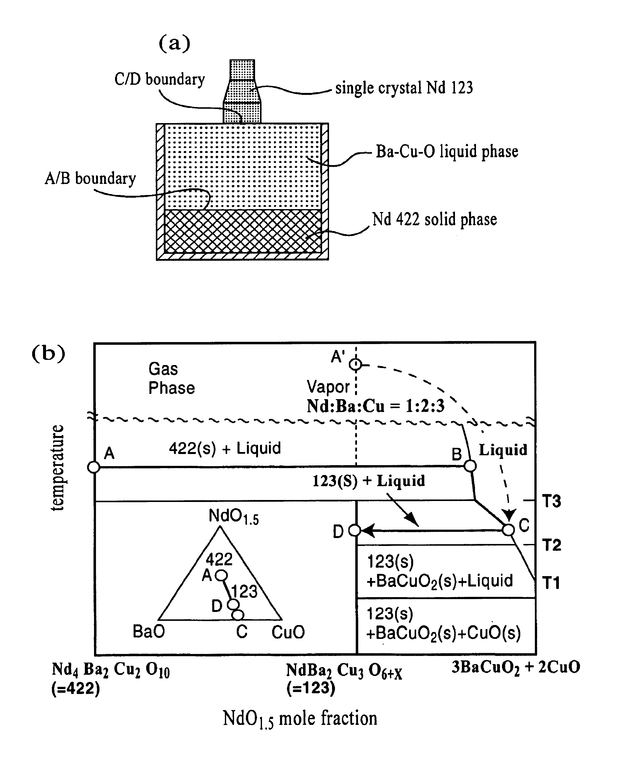
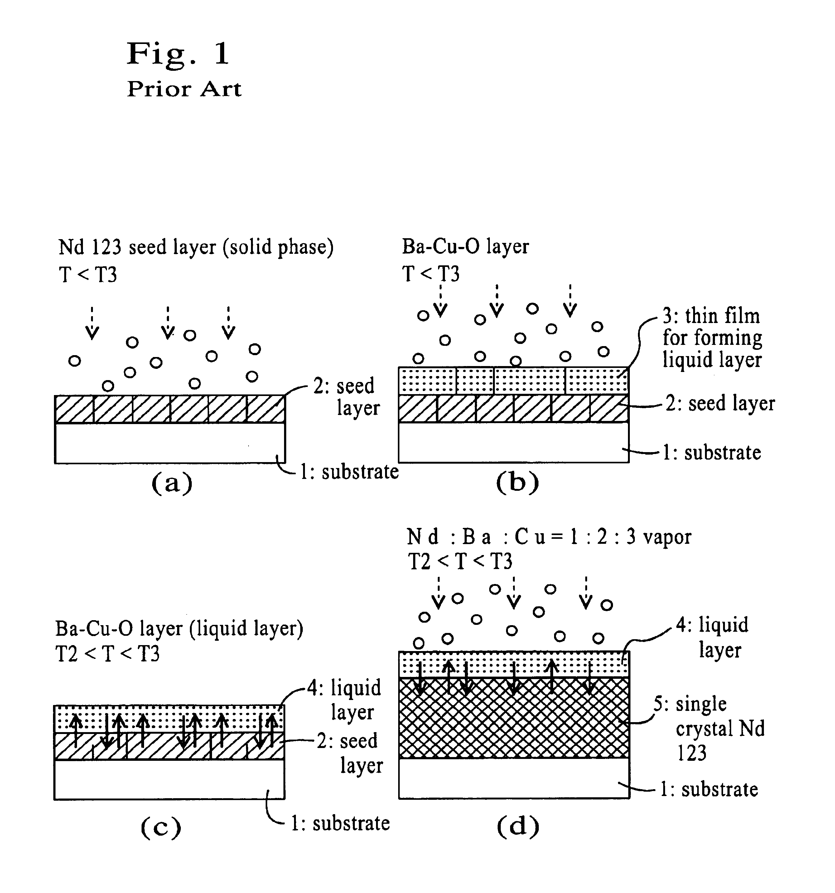
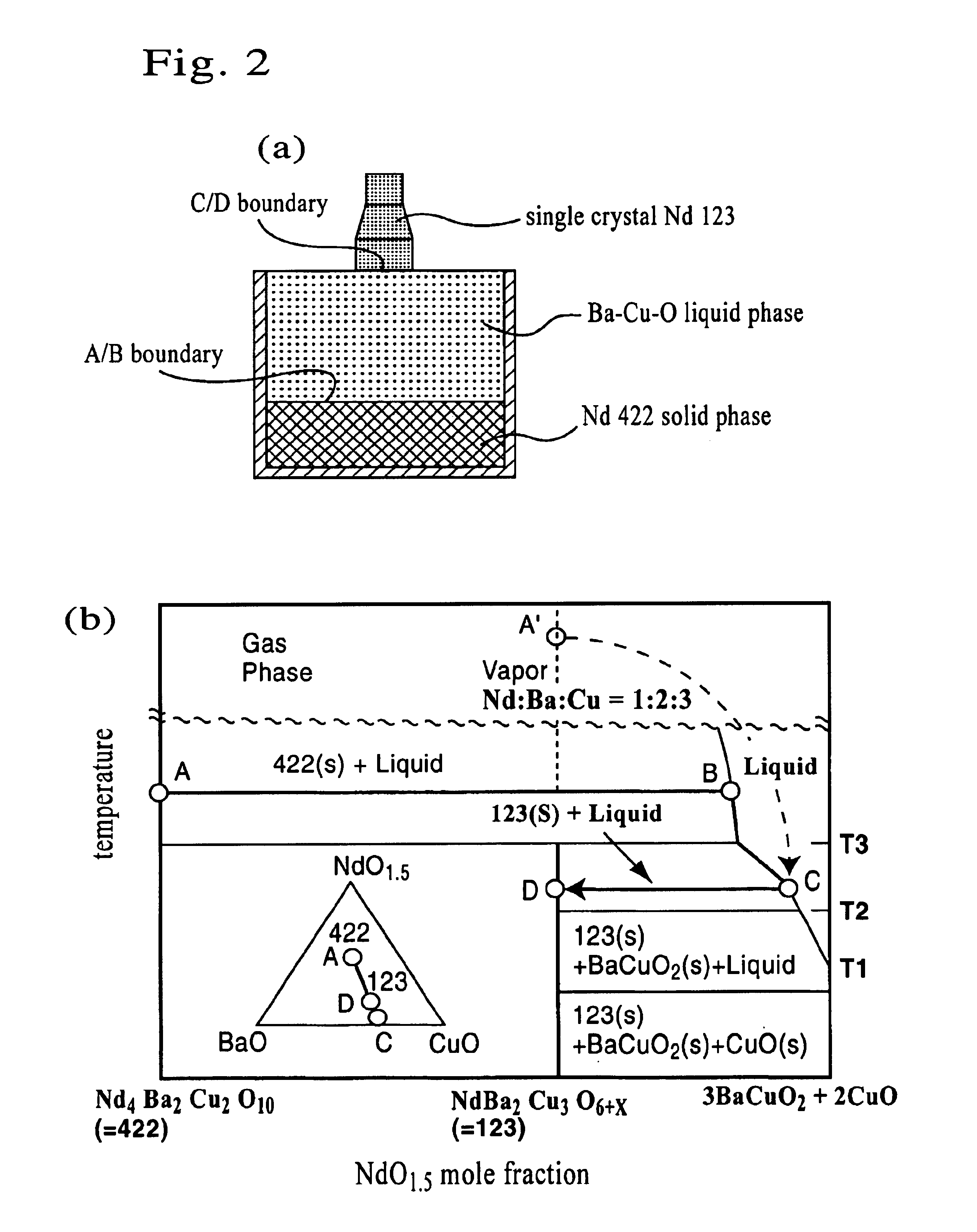
TECHNICAL FIELD[0001]The present invention relates to a method of preparing a single crystal oxide thin film, particularly a high-temperature superconducting thin film of ReBa2Cu3O7 (Re: Y, Nd or Pr) usable for superconductive devices.BACKGROUND ART[0002]When a conventional physical vapor deposition (PVD) method or a non-thermodynamical equilibrium process, such as a sputtering method or a pulsed laser deposition (PLD) method is used to prepare a multicomponent oxide thin film, undesirable defects or precipitations are inevitably introduced in the inside of the thin film. Such defects or precipitations will present a serious hazard to developments of high-temperature superconducting devices such as superconducting tunnel junction devices or microwave devices.[0003]In order to solve this problem, the inventors proposed a new method of growing an epitaxial thin film under three phases: solid phase (a seed layer), liquid phase (liquid layer on the seed layer) and gas phase (gas serving...

Claims


Application Information

Patent Timeline
Patent Type & Authority Patents(United States)
IPC IPC(8): C30B25/02C30B23/02C30B19/00C30B19/04H01L39/24C30B29/22H10N60/01
CPCC30B19/04C30B23/02C30B25/02H01L39/2438C30B29/22C30B29/225C30B23/002H10N60/0436
Inventor KOINUMA, HIDEOMIKAWASAKI, MASASHIMATSUMOTO, YUJI
Owner JAPAN SCI & TECH CORP
Learn More