Semiconductor memory device having a resistance adjustment unit
a technology of resistance adjustment unit and memory device, which is applied in the direction of static storage, digital storage, instruments, etc., can solve the problems of gate and drain bias conditions, affecting the operation of high-speed read operations, and affecting the reliability of data read operations, so as to achieve high speed and high reliability. the effect of data read operations
- Summary
- Abstract
- Description
- Claims
- Application Information
AI Technical Summary
Benefits of technology
Problems solved by technology
Method used
Image
Examples
first embodiment
[First Embodiment]
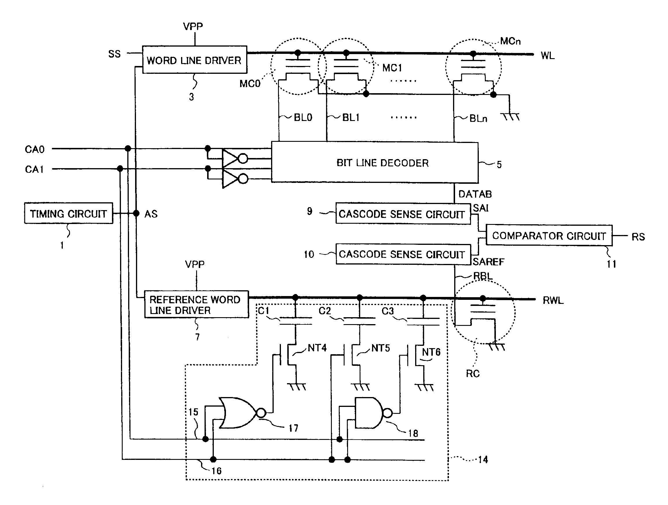
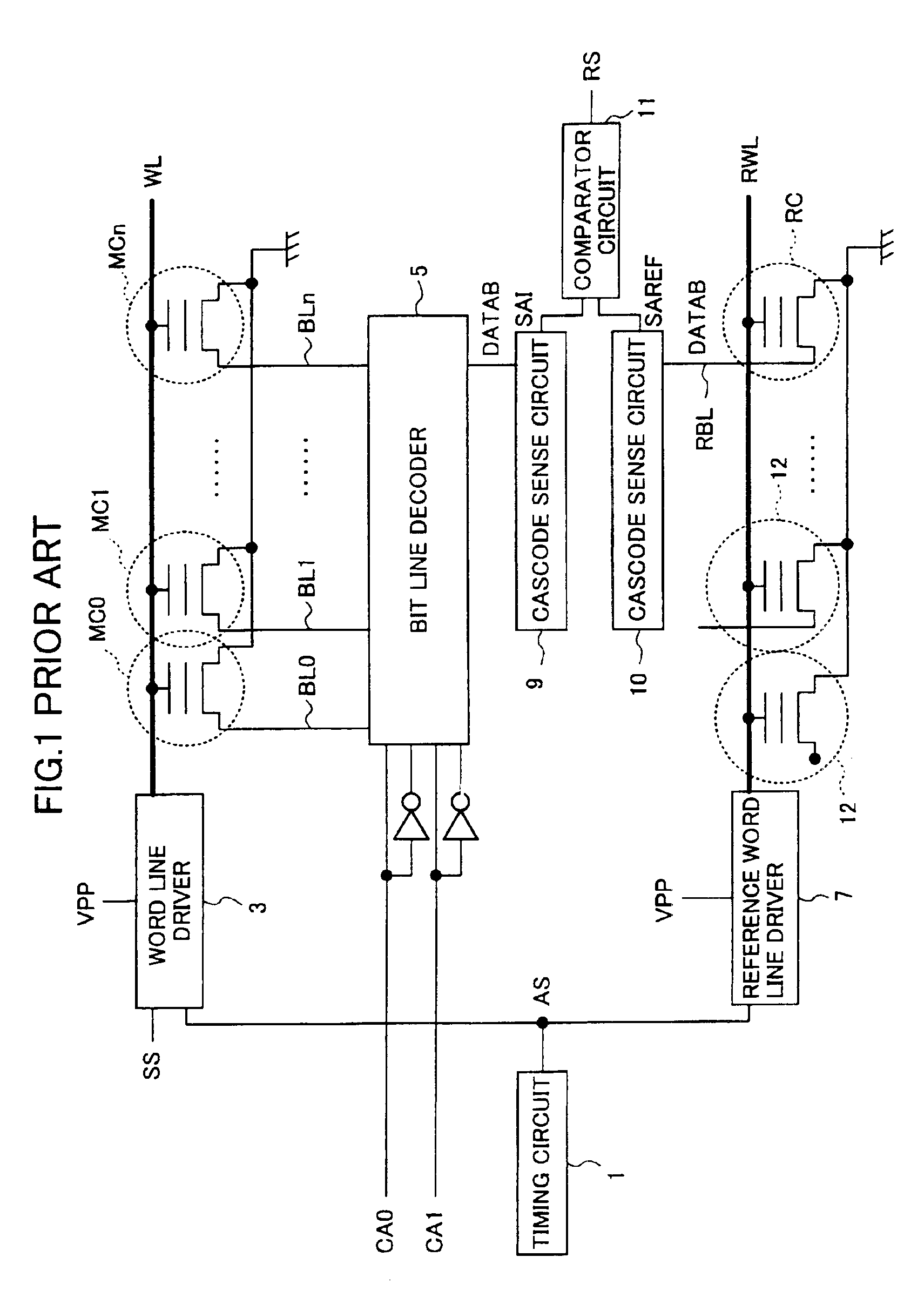
[0059]FIG. 5 is a circuit diagram showing the structure of a nonvolatile semiconductor memory device in accordance with a first embodiment of the present invention. As shown in FIG. 5, the nonvolatile semiconductor memory device of this embodiment differs from the conventional nonvolatile semiconductor memory device shown in FIG. 1 in that the dummy cells 12 are replaced by a load capacity adjustment circuit 14. As shown in FIG. 5, this load capacity adjustment circuit 14 comprises signal lines 15 and 16, an OR circuit 17, an AND circuit 18, capacity elements C1, C2, and C3, and n-channel MOS transistors NT4 to NT6.
[0060]The signal line 15 transmits the column address signal CA0, and the signal line 16 transmits the column address signal CA1. The OR circuit 17 and the AND circuit 18 are connected to the signal lines 15 and 16, and one of the electrodes of each of the capacity elements C1, C2, and C3 is connected to the reference word line RWL. The gate of the n-cha...
second embodiment
[Second Embodiment]
[0065]A nonvolatile semiconductor memory device in accordance with a second embodiment of the present invention has substantially the same structure as the nonvolatile semiconductor memory device of the first embodiment, except that the load capacity adjustment circuit 14 is replaced with a load resistance adjustment circuit 19.
[0066]In the following, the load resistance adjustment circuit 19 will be described in detail. FIG. 6 is a circuit diagram showing a part of the structure of the nonvolatile semiconductor memory device of the second embodiment of the present invention. As shown in FIG. 6, the load resistance adjustment circuit 19 comprises an OR circuit 17, an AND circuit 18, and p-channel MOS transistors PT2 to PT5 and an n-channel MOS transistor NT14 all connected in parallel between the reference word line driver 7 and the reference word line RWL.
[0067]Here, the gate of the p-channel MOS transistor PT2 is grounded, the gate of the p-channel MOS transisto...
third embodiment
[Third Embodiment]
[0073]A nonvolatile semiconductor memory device in accordance with a third embodiment of the present invention has substantially the same structure as the nonvolatile semiconductor memory device of the first embodiment, except that the load capacity adjustment circuit 14 shown in FIG. 5 is replaced with a driver size adjustment circuit 20.
[0074]In the following, the driver size adjustment circuit 20 will be described in detail. FIG. 7 is a circuit diagram showing a part of the structure of the nonvolatile semiconductor memory device of the third embodiment. As shown in FIG. 7, the driver size adjustment circuit 20 comprises the OR circuit 17, the AND circuit 18, and p-channel MOS transistors PT6 to PT8 connected in parallel between the reference word line RWL and a node Npp that supplies the word line booster voltage VPP.
[0075]The gate of the p-channel MOS transistor PT6 is connected to the output node of the OR circuit 17, and the gate of the P-channel MOS transis...
PUM
 Abstract
Description
Claims
Application Information
 - R&D
- Intellectual Property
- Life Sciences
- Materials
- Tech Scout
- Unparalleled Data Quality
- Higher Quality Content
- 60% Fewer Hallucinations
Browse by: Latest US Patents, China's latest patents, Technical Efficacy Thesaurus, Application Domain, Technology Topic, Popular Technical Reports.
© 2025 PatSnap. All rights reserved.Legal|Privacy policy|Modern Slavery Act Transparency Statement|Sitemap|About US| Contact US: help@patsnap.com


