
Semiconductor device

a technology of semiconductor chips and semiconductors, applied in the field of semiconductor devices, can solve problems such as cracks or damage, warpage of substrates, and damage described, and achieve the effects of preventing warpage in substrates, reducing the cost of semiconductor chips, and high elastic modulus

Inactive Publication Date: 2010-07-20
SUMITOMO BAKELITE CO LTD
View PDF12 Cites 1 Cited by
  • Summary
  • Abstract
  • Description
  • Claims
  • Application Information

AI Technical Summary

Benefits of technology

The present invention provides a semiconductor device that minimizes warpage of the substrate and prevents damage to the semiconductor chip and bump connections. This is achieved by using an underfill made of a resin material with a high elastic modulus that fixes the periphery of the bump and prevents cracks. The substrate and semiconductor chip have low linear expansion coefficients, reducing warpage in the substrate and preventing damage to the chip. The elastic modulus of the underfill is determined under an atmosphere of 125°C.

Problems solved by technology

Therefore, when a semiconductor device having a structure that a semiconductor chip is mounted on a substrate is subjected to heat history, a difference in a linear expansion coefficient between them causes warpage of the substrate.
It is known that in a conventional semiconductor device, such warpage may cause cracks or damage in, for example, a semiconductor chip, an interface between a semiconductor chip and a bump, or an interface between a bump and a substrate.
In addition, warpage of a package in which a semiconductor chip is mounted on a substrate causes not only the damage described above but also difficulty in mounting a package on a substrate.

Method used


Image

  • Semiconductor device
  • Semiconductor device
  • Semiconductor device

Examples


example 1

[0075]The present invention will be detailed with reference to Examples and Comparative Examples, but the present invention is not limited to them.

[0076]First, an underfill material used in this example will be described.

example 1-1

[0077]Preparation of a resin composition: 13.5 parts by weight of bisphenol-F type epoxy resin (epoxy equivalent: 165), 13.5 parts by weight of[0078]N-[2-methyl-4-(oxiranylmethoxy)phenyl]-N-(oxiranylmethyl)oxiraneme thanamine (Sumitomo Chemical Co., Ltd., ELM-100), 13 parts by weight of 4,4′-methylenebis-(2-ethylaniline) (Nippon Kayaku Co., Ltd., KAYAHARD AA), 1 part by weight of γ-glycidylpropyltriethoxysilane and 65 parts by weight of spherical fused silica SO-25R (Admatechs Co., Ltd.) were weighed and kneaded by a three-roll mill, to prepare a liquid resin composition after degassing in vacuo.

example 1-2

[0079]A procedure was conducted as described in Example 1-1, except that the following resin composition was used. That is, were used 18 parts by weight of bisphenol-F type epoxy resin (epoxy equivalent: 165), 6 parts by weight of[0080]N-[2-methyl-4-(oxiranylmethoxy)phenyl]-N-(oxiranylmethyl)oxiraneme thanamine (Sumitomo Chemical Co., Ltd., ELM-100) and 10 parts by weight of 4,4′-methylenebis-(2-ethylaniline) (Nippon Kayaku Co., Ltd., KAYAHARD AA).


PUM


Abstract

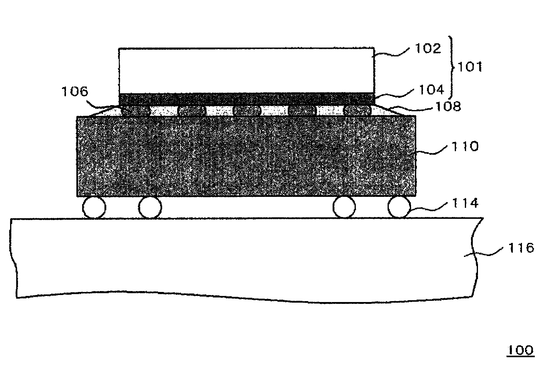
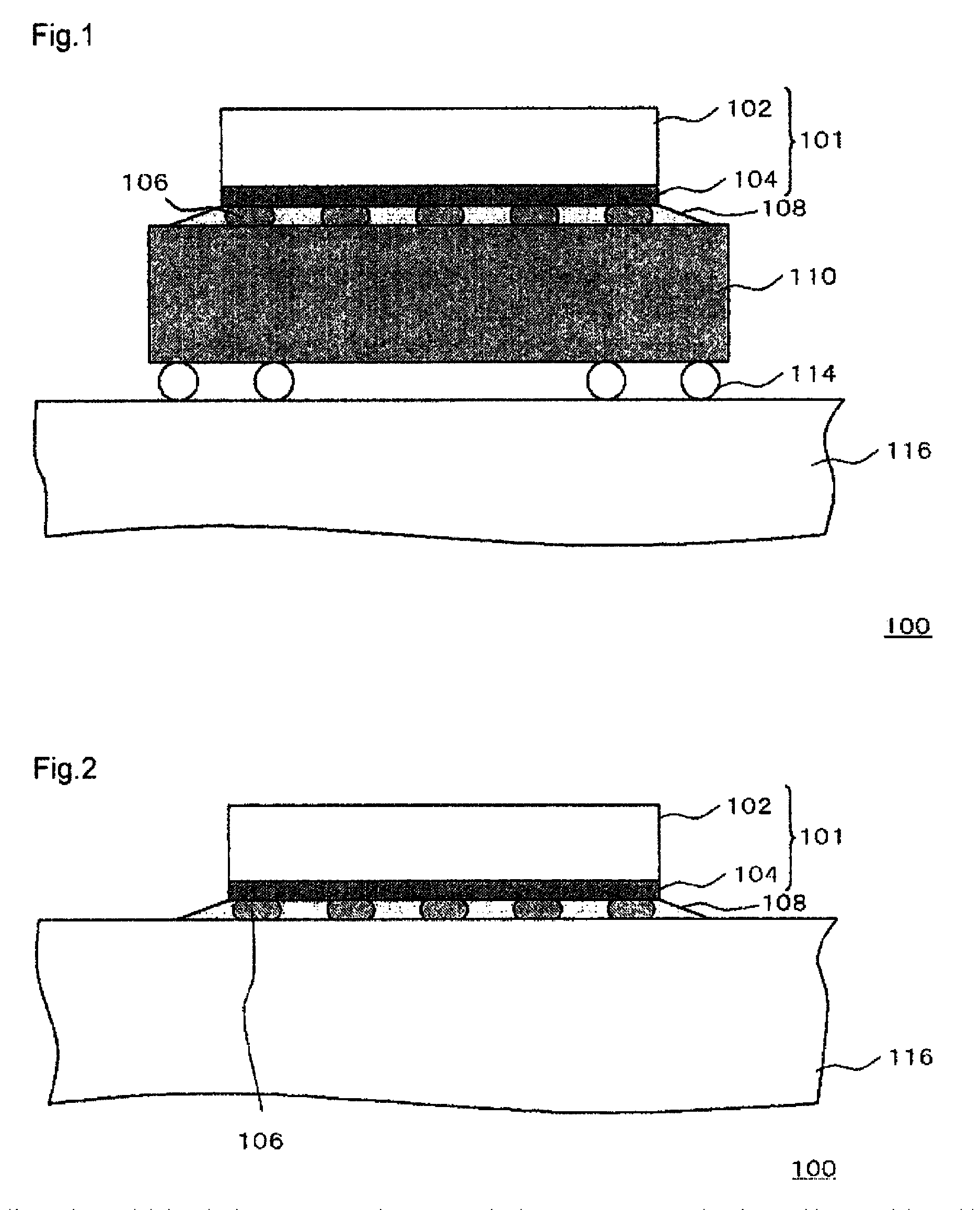
A semiconductor device 100 has a BGA substrate 110, a semiconductor chip 101, a bump 106 and an underfill 108 filling the periphery of the bump. An interlayer dielectric 104 in the semiconductor chip 101 contains a low dielectric constant film. The bump 106 is comprised of a lead-free solder. The underfill 108 is comprised of a resin material having an elastic modulus of 150 MPa to 800 MPa both inclusive, and a linear expansion coefficient of the BGA substrate 110 in an in-plane direction of the substrate is less than 14 ppm / ° C.

Description

TECHNICAL FIELD[0001]The present invention relates to a semiconductor device where a semiconductor chip is mounted on a substrate.BACKGROUND ART[0002]When a semiconductor chip is face-down mounted on a substrate, a gap is formed between the substrate and the chip, so that the gap must be filled with an insulating material called an underfill. A commonly used underfill has been conventionally a thermosetting resin represented by an epoxy resin (Patent Document 1).Patent Document 1: Japanese Laid-open Patent Publication No. 11-233571DISCLOSURE OF THE INVENTION[0003]A semiconductor device in which a semiconductor chip is face-down mounted has the following problems.[0004]A linear expansion coefficient is generally different between a substrate and a semiconductor chip. A substrate is made of a material containing an organic resin, which has a larger linear expansion coefficient than a semiconductor chip. Therefore, when a semiconductor device having a structure that a semiconductor chi...

Claims


Application Information

Patent Timeline
Patent Type & Authority Patents(United States)
IPC IPC(8): H01L23/48H01L23/29
CPCH01L21/563H01L23/14H01L23/5329H01L24/81H01L2924/3511H01L2924/1434H01L2924/1431H01L2924/10253H01L2224/73204H01L2224/32225H01L2224/29386H01L2224/2929H01L2224/16225H01L2224/13139H01L2224/13111H01L24/73H01L23/5222H01L2224/8121H01L2224/81815H01L2924/01012H01L2924/01013H01L2924/01015H01L2924/0102H01L2924/01022H01L2924/01027H01L2924/01029H01L2924/0103H01L2924/01033H01L2924/01059H01L2924/01061H01L2924/01073H01L2924/01077H01L2924/01078H01L2924/01082H01L2924/04953H01L2924/15311H01L2924/01006H01L2924/01019H01L2924/01047H01L2924/0105H01L2924/014H01L24/13H01L24/16H01L24/29H01L24/32H01L2924/00012H01L2924/01083H01L2924/00H01L2224/05085H01L23/48
Inventor SUGINO, MITSUOHOSOMI, TAKESHISAKAMOTO, YUSHI
Owner SUMITOMO BAKELITE CO LTD
Learn More