Bank address mapping according to bank retention time in dynamic random access memories
a random access memory and bank address technology, applied in memory architecture accessing/allocation, program control, sustainable buildings, etc., can solve the problems of data destruction in drams, high power consumption of computing systems using dram,
- Summary
- Abstract
- Description
- Claims
- Application Information
AI Technical Summary
Problems solved by technology
Method used
Image
Examples
Embodiment Construction
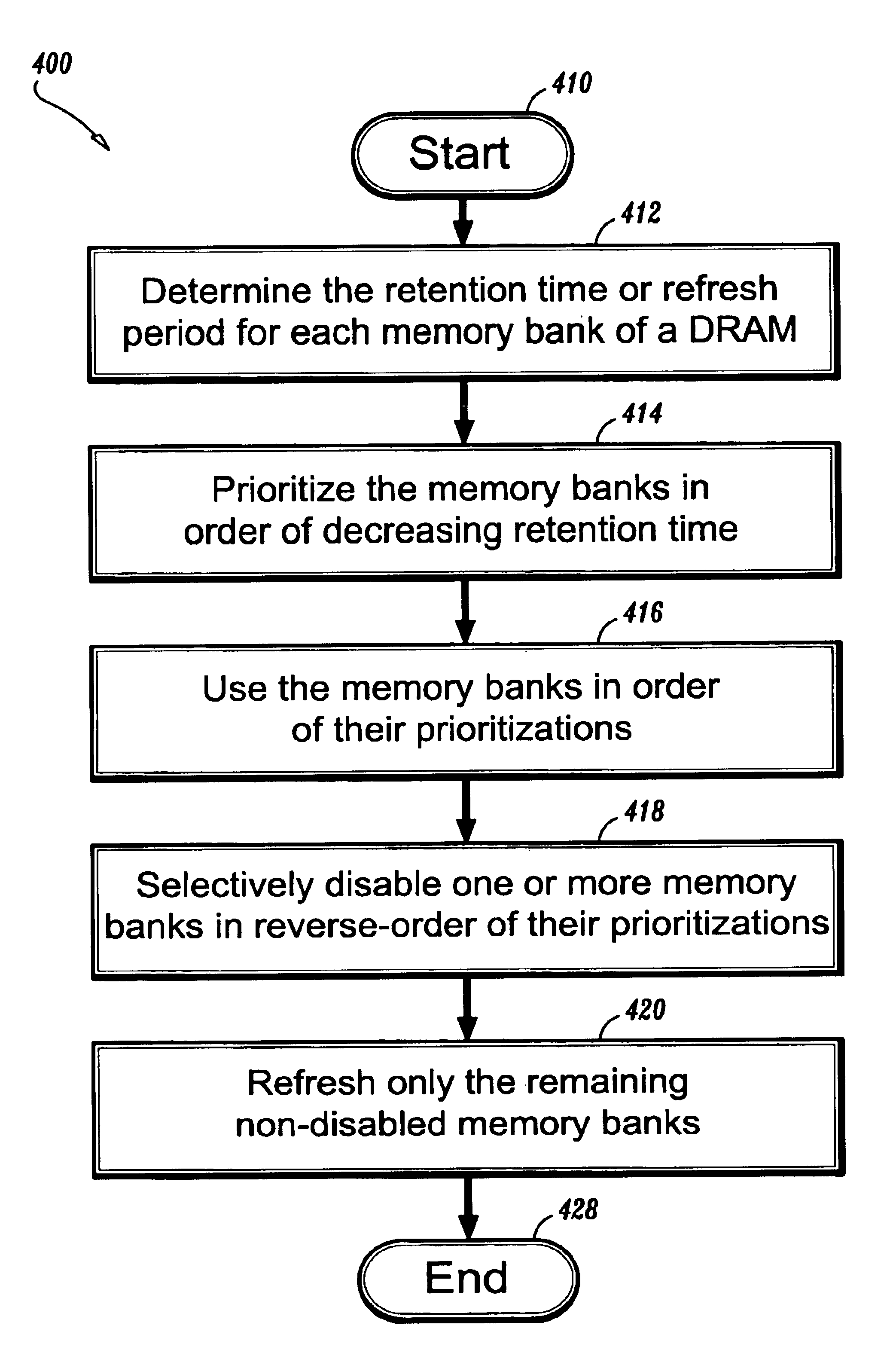
[0015]A system and method are provided for mapping memory bank addresses relative to memory bank retention times in dynamic random access memories (“DRAMs”). Battery-powered mobile computing systems, for example, typically have a power-down mode to reduce power consumption by the display and / or other peripheral devices during periods of low usage. Thus, the present disclosure presents a system and method to further reduce the power consumption of a DRAM device. A feature referred to as a “partial array self-refresh” has been introduced in mobile DRAMs. This feature allows the DRAM chip to refresh only selected banks during a power-down mode. Either one bank, two banks or all banks may be activated and refreshed during the power-down mode. Non-activated banks are not refreshed, and are permitted to lose their data.
[0016]As the array sizes of current DRAM chips continue to be increased, the likelihood of having banks with different retention times is also increased. Thus, to further m...
PUM
 Abstract
Description
Claims
Application Information
 - R&D
- Intellectual Property
- Life Sciences
- Materials
- Tech Scout
- Unparalleled Data Quality
- Higher Quality Content
- 60% Fewer Hallucinations
Browse by: Latest US Patents, China's latest patents, Technical Efficacy Thesaurus, Application Domain, Technology Topic, Popular Technical Reports.
© 2025 PatSnap. All rights reserved.Legal|Privacy policy|Modern Slavery Act Transparency Statement|Sitemap|About US| Contact US: help@patsnap.com


