Magneto-resistive device with a magnetic multilayer structure
- Summary
- Abstract
- Description
- Claims
- Application Information
AI Technical Summary
Benefits of technology
Problems solved by technology
Method used
Image

Examples
Embodiment Construction
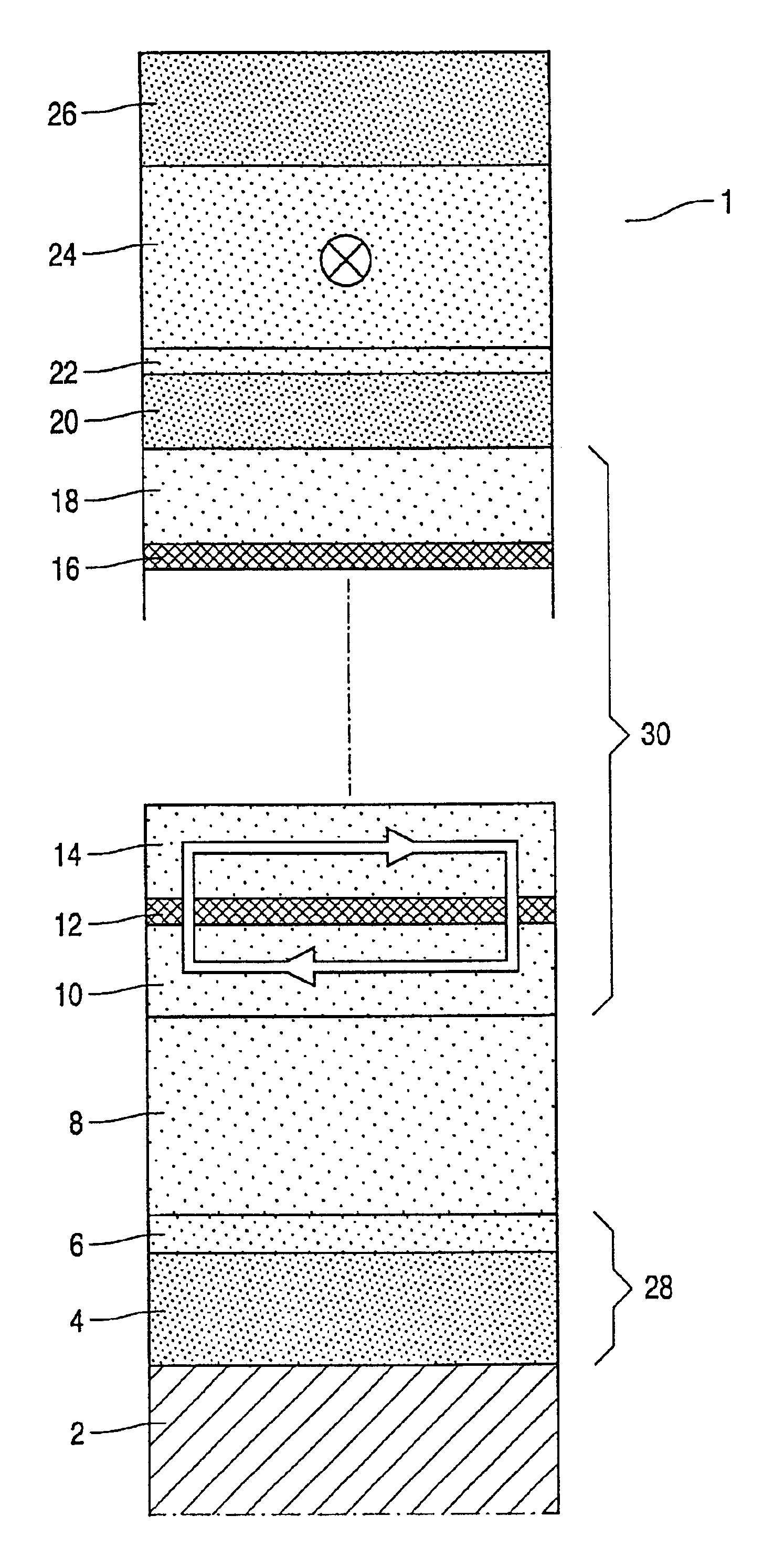
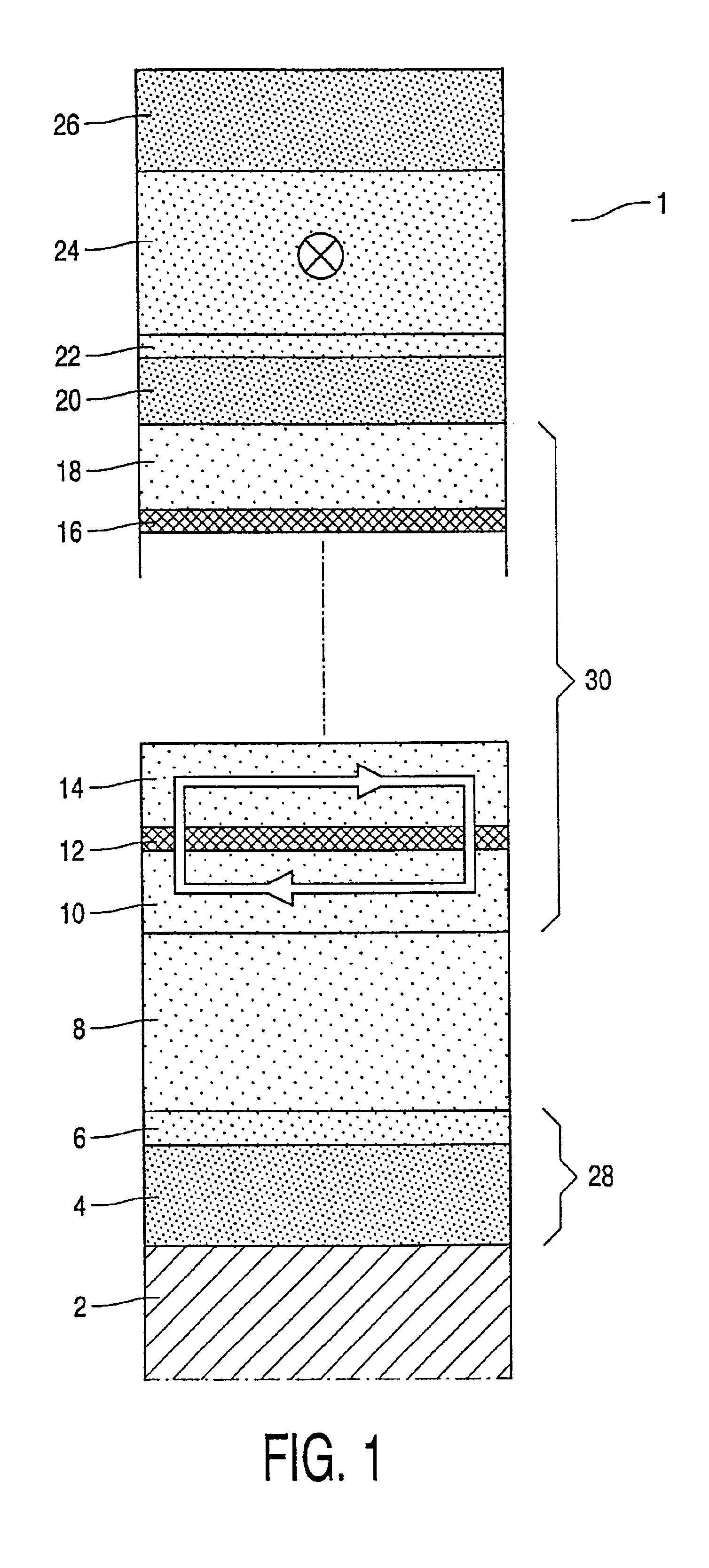
[0023]The present invention will be described with reference to certain embodiments and with reference to certain drawings but the present invention is not limited thereto but only by the claims. In particular embodiments of the invention of magnetic multilayer configurations based on a basic GMR- or TMR-stack are disclosed. These multilayer configurations can be integrated in the systems of the invention according to techniques known to the person of skill in the art. It is for example possible in an embodiment of the invention to integrate the whole sensing or data storage system on one semiconductor (silicon) chip with the multilayer configuration being grown or deposited on the chip. The multilayer configuration can be grown or deposited on the chip in the front-end or in the back-end of the process for making the chip. In the back-end process a part of the chip is planarized and the multilayer configuration is deposited or grown thereon. Appropriate connections by bonding or vi...
PUM
 Abstract
Description
Claims
Application Information
 - R&D
- Intellectual Property
- Life Sciences
- Materials
- Tech Scout
- Unparalleled Data Quality
- Higher Quality Content
- 60% Fewer Hallucinations
Browse by: Latest US Patents, China's latest patents, Technical Efficacy Thesaurus, Application Domain, Technology Topic, Popular Technical Reports.
© 2025 PatSnap. All rights reserved.Legal|Privacy policy|Modern Slavery Act Transparency Statement|Sitemap|About US| Contact US: help@patsnap.com