
One transistor SOI non-volatile random access memory cell

a random access memory cell, non-volatile technology, applied in the field of integrated circuits, can solve the problems of volatile dram device, permanent data loss in dram device, difficult manufacturing,

Inactive Publication Date: 2005-05-03
MICRON TECH INC
View PDF41 Cites 120 Cited by
  • Summary
  • Abstract
  • Description
  • Claims
  • Application Information

AI Technical Summary

Benefits of technology

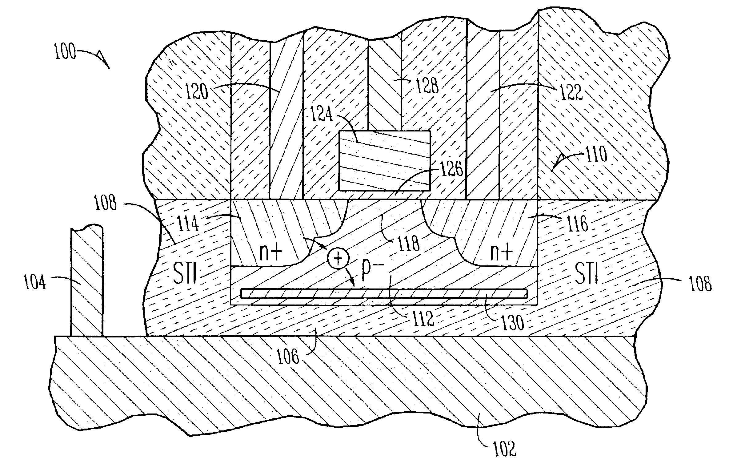
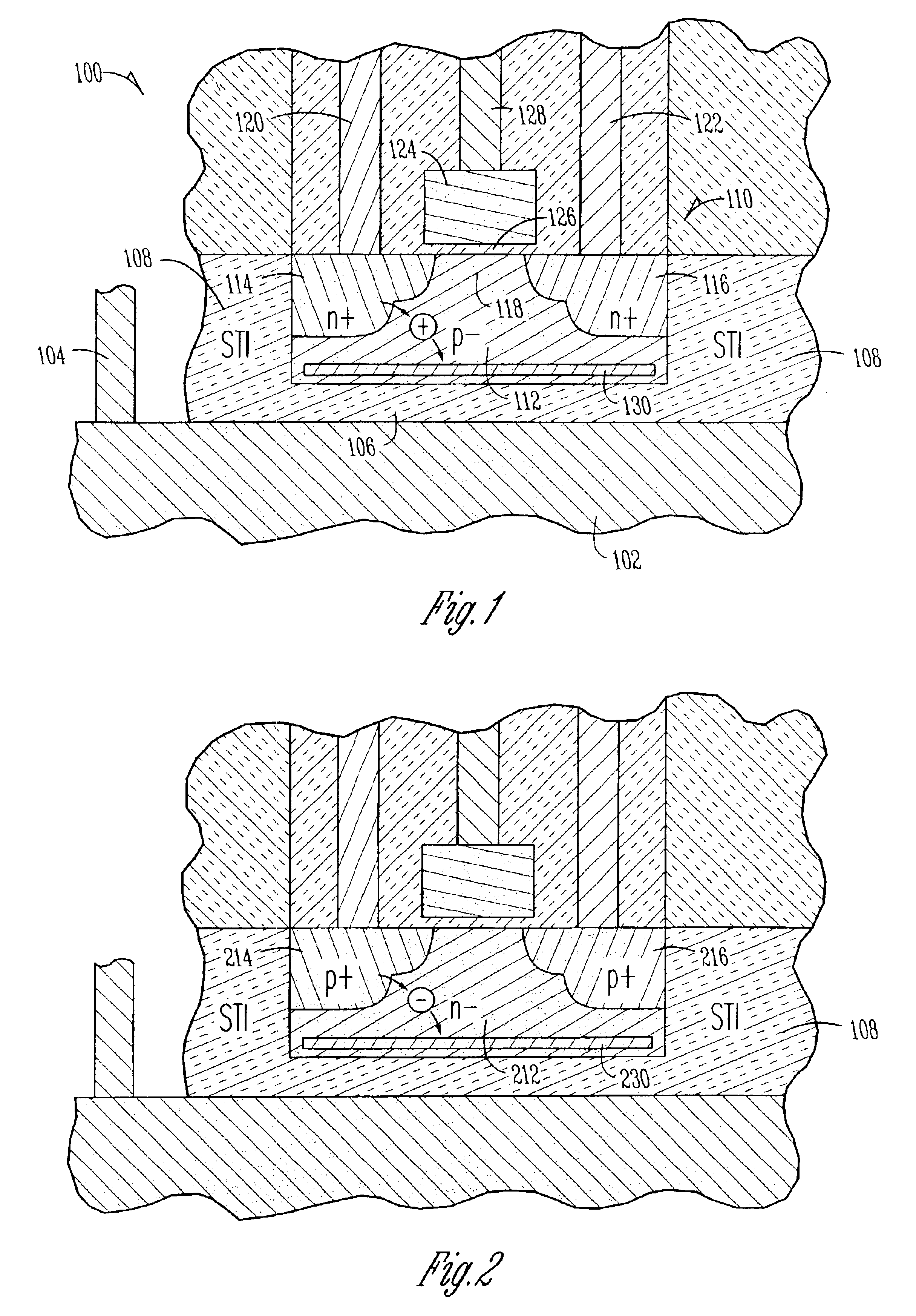
The present subject matter is about non-volatile memory cells that use a transistor with a floating body that contains charge traps. The transistor can trap charges in the floating body to create a stable binary memory state. The charges can be neutralized or de-trapped to change the memory state. The memory cell has a long charge retention and non-volatility. It also has high density and fast read-write capabilities. The transistor includes a charge trapping region near the interface between the transistor body and the buried insulator, which can be neutralized by providing charges of opposite polarity. The memory cell can provide a stable memory state and can be used in various electronic devices.

Problems solved by technology

Thus, such a DRAM device is volatile.
A power failure causes permanent data loss in a DRAM device.
A significant challenge for every succeeding generation of reduced feature size is to provide this minimum capacitance per cell.
However, these complex three-dimensional capacitor structures are difficult to manufacture and adversely impact yield.
There has been serious concern of the scalability of the conventional DRAM cell beyond the 0.1 μm lithographic generation.
The scaling problems have been aggravated by increased device short channel effects and leakages associated with complicated capacitor structures.
Therefore, controlling the memory retention between refresh operations is expected to be difficult.
Field emission across the surrounding insulator causes the stored charge to leak.
However, there are problems associated with NVRAM devices.
The writing process, also referred to as “write-erase programming,” for non-volatile memory is slow and energy inefficient, and requires complex high voltage circuitry for generating and routing high voltage.
The degradation of the insulator eventually causes significant leakage of the stored charge.
Thus, the high-field phenomena negatively affects the endurance (the number of write / erase cycles) of the NVRAM devices.
Therefore, the available applications for these known NVRAM devices is limited.

Method used


Image

  • One transistor SOI non-volatile random access memory cell
  • One transistor SOI non-volatile random access memory cell
  • One transistor SOI non-volatile random access memory cell

Examples


Embodiment Construction

[0041]The following detailed description refers to the accompanying drawings which show, by way of illustration, specific aspects and embodiments in which the present subject matter may be practiced. These embodiments are described in sufficient detail to enable those skilled in the art to practice the present subject matter. The various embodiments of the present subject matter are not necessarily mutually exclusive. Other embodiments may be utilized and structural, logical, and electrical changes may be made without departing from the scope of the present subject matter. In the following description, the terms wafer and substrate are interchangeably used to refer generally to any structure on which integrated circuits are formed, and also to such structures during various stages of integrated circuit fabrication. Both terms include doped and undoped semiconductors, epitaxial layers of a semiconductor on a supporting semiconductor or insulating material, combinations of such layers...


PUM


Abstract

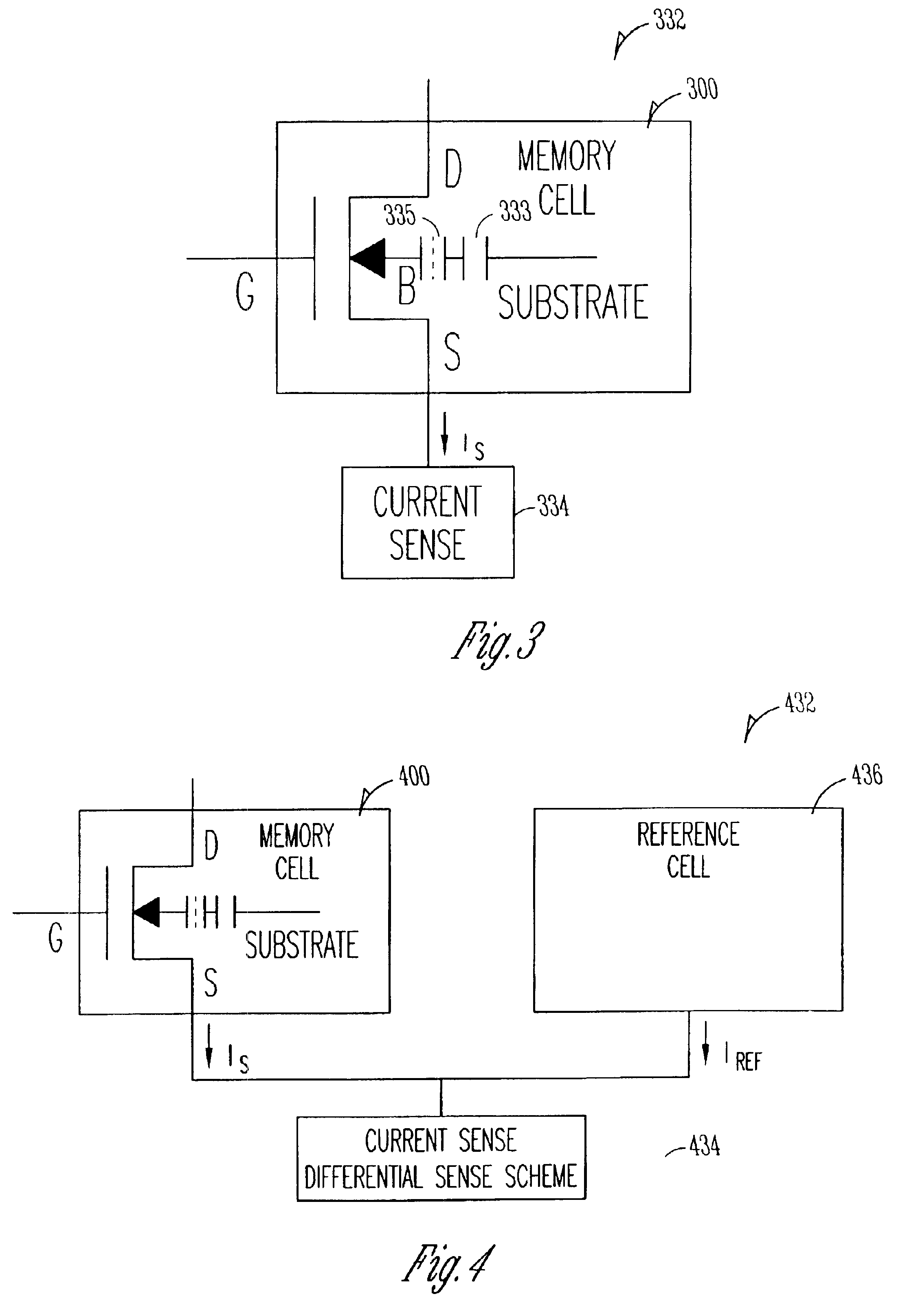
One aspect of the present subject matter relates to a memory cell, or more specifically, to a one-transistor SOI non-volatile memory cell. In various embodiments, the memory cell includes a substrate, a buried insulator layer formed on the substrate, and a transistor formed on the buried insulator layer. The transistor includes a floating body region that includes a charge trapping material. A memory state of the memory cell is determined by trapped charges or neutralized charges in the charge trapping material. The transistor further includes a first diffusion region and a second diffusion region to provide a channel region in the body region between the first diffusion region and the second diffusion region. The transistor further includes a gate insulator layer formed over the channel region, and a gate formed over the gate insulator layer. Other aspects are provided herein.

Description

CROSS REFERENCE TO RELATED APPLICATIONS[0001]This application is a Continuation-in-Part of U.S. Ser. No. 10 / 232,846, filed on Aug. 30, 2002, which is incorporated herein by reference in its entirety.[0002]This application is related to the following commonly assigned U.S. patent applications which are herein incorporated by reference in their entirety: “Scalable Flash / NV Structures & Devices With Enhanced Endurance,” U.S. application Ser. No. 09 / 944,985, filed on Aug. 30, 2001; “Stable PD-SOI Devices and Methods,” U.S. application Ser. No. 10 / 197,978, filed on Jul. 18, 2002; “Gated Lateral Thyristor-Based Random Access Memory Cell (GLTRAM),” U.S. application Ser. No. 10 / 232,855, filed on Aug. 30, 2002; and “One-Device Non-Volatile Random Access Memory Cell,” U.S. application Ser. No. 10 / 232,848, filed on Aug. 30, 2002.TECHNICAL FIELD[0003]This disclosure relates generally to integrated circuits, and more particularly, to non-volatile, silicon-on-insulator (SOI) memory cells.BACKGROU...

Claims


Application Information

Patent Timeline
Patent Type & Authority Patents(United States)
IPC IPC(8): H01L29/66H01L29/788H01L29/792
CPCG11C16/0466H01L27/108H01L29/792H01L29/66833H01L29/7841H01L29/78612H01L29/7881H01L27/10802G11C7/062G11C2207/063G11C2211/4016H10B12/20H10B12/00
Inventor BHATTACHARYYA, ARUP
Owner MICRON TECH INC
Learn More