
Methods of optical filament scribing of circuit patterns with planar and non-planar portions

a technology of optical filament and circuit pattern, applied in the field of optical filament circuit board, can solve the problems of difficult to manufacture commercial interconnection cards with optical filaments, difficult to provide with known electrically wired backplanes, and difficult to control the size of optical filaments, etc., and achieves the effect of convenient mass production, low cost and quick delivery

Inactive Publication Date: 2005-04-26
STRATOS INT
View PDF23 Cites 16 Cited by
  • Summary
  • Abstract
  • Description
  • Claims
  • Application Information

AI Technical Summary

Benefits of technology

This approach enables faster and more robust scribing of optical filament circuit boards, reducing breakage and stress on the filaments, facilitating mass production with stronger bond strengths and smoother surfaces suitable for further processing, such as printing.

Problems solved by technology

For example, optical backplanes increasingly are used in electronics systems where greater circuit density is desired, but is difficult to provide with known electrically wired backplanes.
However, commercial interconnection card manufacture with optical filaments is difficult and these known methods often lead to unacceptable results.
Optical filaments are extremely small and difficult to handle.
These tiny filaments also are fragile, and often cannot withstand stresses attendant to abrupt turns or the like during the scribing process.
Optical filament breakage at crossovers (i.e., where one wire overlaps itself or another wire) is particularly problematic, because stresses at these points can increase dramatically.
This can be even more troublesome when ultrasonic energy is used to adhere the filaments to the substrate, which can lead to further filament breakage.
However, during wire scribing, the stresses can be so severe (reaching up to up to 12 MPa at crossovers) that the wire conductor ruptures.
Similarly, the stress on optical filaments during scribing increases the possibility of breakage, and “microbending,” a condition that causes signal attenuation along the optical filament.
However, the '230 patent and the '818 patent fail to describe a single embodiment using optical filaments or provide process parameters for successfully scribing optical filaments according to these methods.
This pressure, which is necessary to encapsulate the optical filaments, also may break the optical filaments.
Breakage is especially a problem at crossovers , which are increasingly common and necessary in optical filament circuit cards.
Again, the fibers in this method still are susceptible to damage, particularly when many crossovers are included in the optical filament circuit pattern, because heat and pressure are applied to the thermoplastic sheet material.
Various machines are available for automatically routing and bonding electrical wire to a substrate, but, in general, these machines cannot be adopted for optical filament use because optical filament is relatively fragile and is relatively unable to withstand heat and pressure, abrupt turns, etc.

Method used


Image

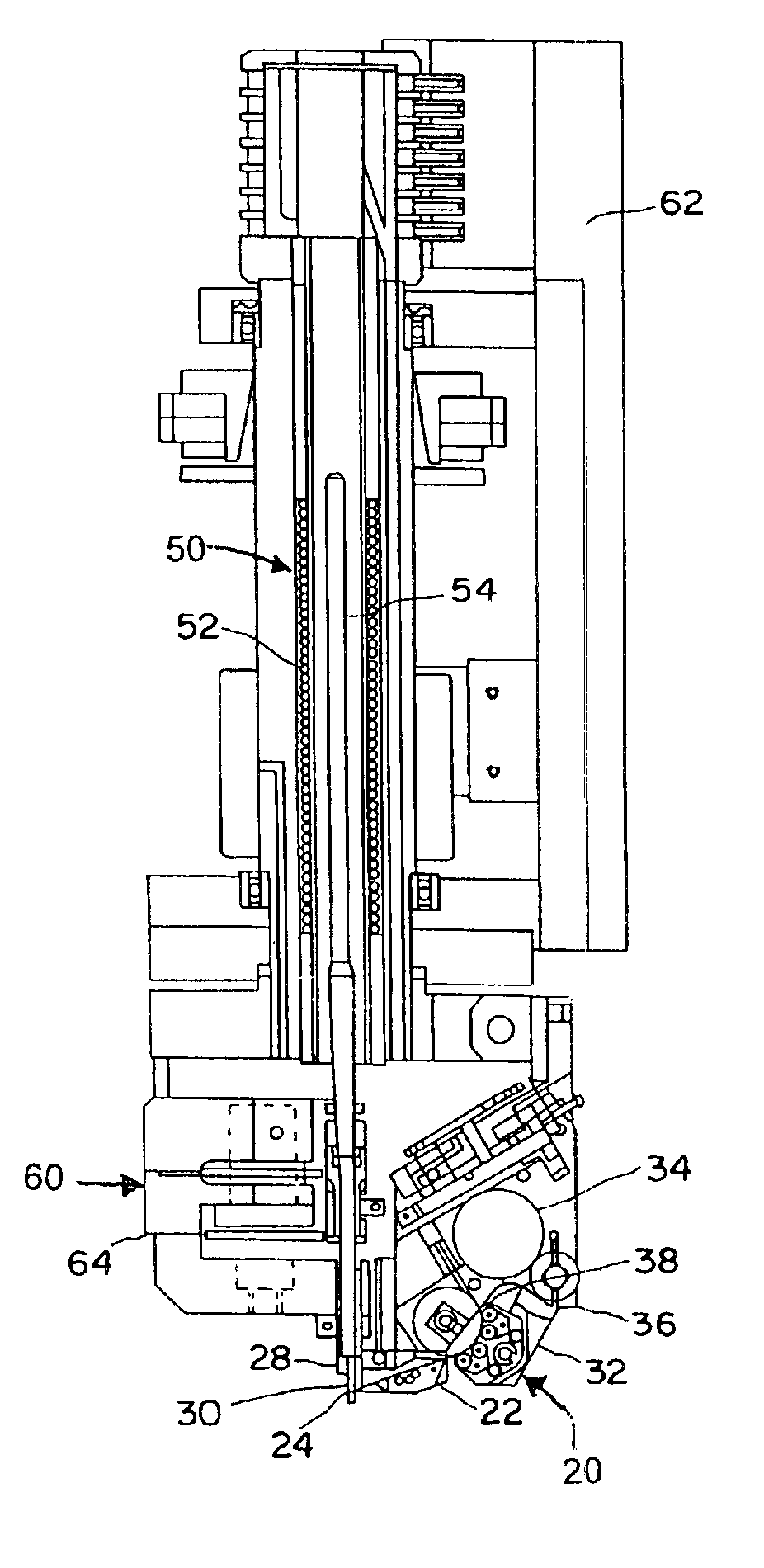
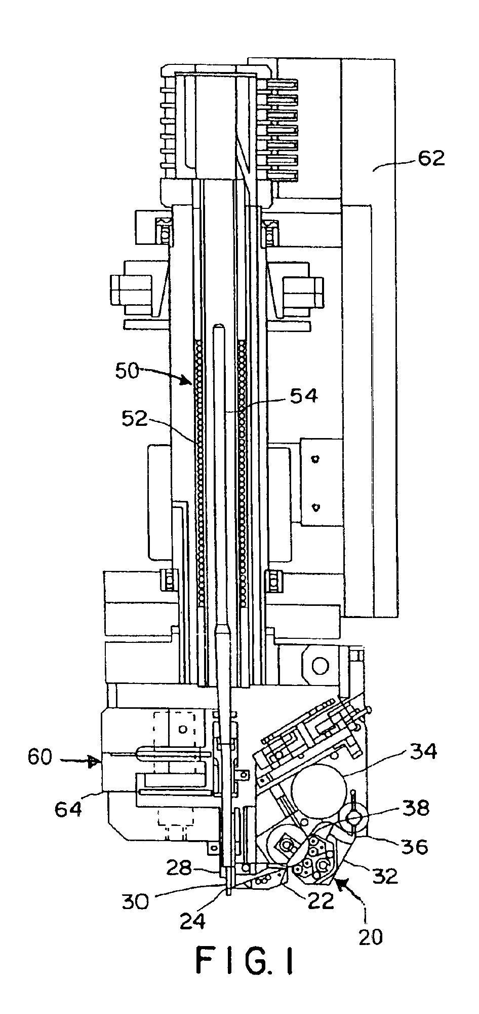
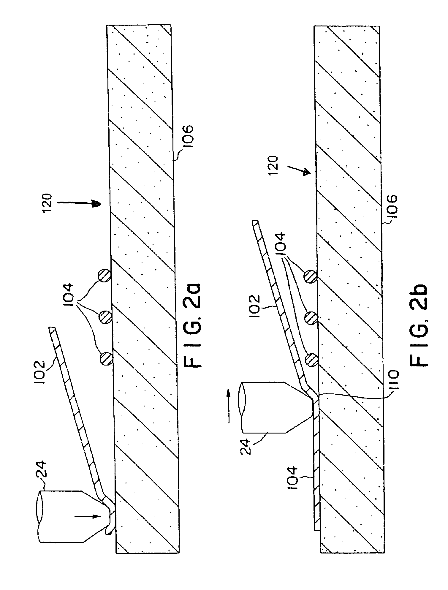
  • Methods of optical filament scribing of circuit patterns with planar and non-planar portions
  • Methods of optical filament scribing of circuit patterns with planar and non-planar portions
  • Methods of optical filament scribing of circuit patterns with planar and non-planar portions

Examples


example 1

[0091]An apparatus as described above is used with optical filament to make a scribed filament circuit pattern with planar and non-planar portions. For example, a COILPRO™ 2000 series wiring machine or a COILPRO™ 4000 series wiring machine, both available from Advanced Interconnection Technology, L.L.C. (a Stratos Lightwave company) of Hauppauge, N.Y., can be used.

[0092]The substrate is a polyimide film commercially available from DuPont, Inc. (Wilmington, Del.) under the trademark KAPTON® 200HN, and is 50 μm thick. The substrate is prepared by bonding a layer of adhesive to one surface. The adhesive is an acrylic resin commercially available from 3M (St. Paul, Minn.) under the trademark VHB™ Adhesive Transfer Tape. The adhesive is 250 μm thick. The adhesive is bonded to the substrate using a roll laminator. To accomplish this, the two films are aligned to one another and passed between the rollers of the laminator. The compliant rollers squeeze the materials together.

[0093]The opti...


PUM

PropertyMeasurementUnit
temperatureaaaaaaaaaa
output poweraaaaaaaaaa

Abstract

Methods of forming optical filament circuit patterns with planar and non-planar portions are provided. An optical filament circuit pattern is scribed by moving a filament guide and a substrate relative to one another at a speed between about 110 inches / minute and about 190 inches / minute, and dispensing an optical filament on, or in the vicinity of, a surface of the substrate. The filament or the substrate or both have adhesive surface(s). The adhesive surface is capable of being adhesively actuated by application of energy. Energy is applied simultaneous with, or subsequent to, scribing. Preferably, ultrasound energy is applied having an output power between about 2.0 watts and about 3.5 watts while applying a pressure to the filament between about 1.177 Newtons and about 1.324 Newtons. A portion of the filament circuit pattern is planar and another portion is non-planar. The non-planar portion traverses but does not contact or adhere to a pre-selected area of the substrate. The pre-selected area corresponds with a pad, a contact pattern, a hole, a slot, a raised feature, a part of the previously scribed planar portion of the pattern, and a filament termination point. Alternately, the non-planar portion may be embedded below the surface of the substrate. Another planar portion of the filament circuit traverses the non-planar portion but does not contact or adhere to a pre-selected part of the previously scribed non-planar portion. Optical filament-scribed circuit boards are formed by this method.

Description

[0001]This application is a continuation-in-part application of U.S. application Ser. No. 09 / 211,511, filed Dec. 14, 1998, now abandoned, the entirety of which is incorporated herein by reference.FIELD OF THE INVENTION[0002]The present invention relates to optical filament circuit boards and methods of their manufacture. More particularly the present invention relates to an improved method of adhering optically conductive filaments onto dielectric substrates to form filament circuit patterns with both planar and non-planar portions and interconnection cards, Smart Cards or optical filament circuit cards formed therefrom.BACKGROUND OF THE INVENTION[0003]In the manufacture and assembly of electric and electronic units, wiring boards have long been used to interconnect electronic components. These “interconnection” boards or cards have an insulating substrate with a plurality of electronic components, which may be integrated circuit packages, or other types of electronic, electro-optic...

Claims


Application Information

Patent Timeline
Patent Type & Authority Patents(United States)
IPC IPC(8): G06K19/077H05K3/10H05K7/02H05K7/06H05K3/46H05K3/38B42D15/10D02JG02B6/02G02B6/13G06K19/00
CPCG02B6/02G02B6/13G06K19/07743H05K3/103H05K7/06H05K2203/1105H05K3/4685H05K2201/10287H05K2203/0285H05K3/386
Inventor KEOGH, RAYMOND S.
Owner STRATOS INT
Learn More