Method of forming a dielectric film

Inactive Publication Date: 2005-03-15
TOKYO ELECTRON LTD
View PDF17 Cites 14 Cited by
  • Summary
  • Abstract
  • Description
  • Claims
  • Application Information

AI Technical Summary

Benefits of technology

Accordingly, it is a general object of the present invention to provide a novel and useful method of forming a dielectric film wherein the foregoing problems are eliminated.
Another and more specific object of the present invention is to provide a method of forming a dielectric film by a vapor phase deposition process without causing damages in the dielectric film by charged particles while minimizing the incubation time for deposition of the dielectric film and simultaneously reducing the surface roughness.
Another object of the present invention is to provide a method of forming a dielectric film by a vapor phase deposition process without causing damages in the dielectric film by charged particles while arbitrarily controlling a compositional profile of the dielectric film in a thickness direction thereof.
According to the present invention, it becomes possible to form a dielectric or high-dielectric film of various compositions including Ta2O5 on a Si substrate by a CVD process with reduced incubation time. As a result, the uniformity of the obtained dielectric film is improved. Further, the present invention enables arbitrary control of composition of the dielectric film in the thickness direction thereof. According to the needs, it is also possible to form an extremely thin diffusion barrier film of about a single molecular layer thickness inside the dielectric film. In view of the fact that the present invention does not include the step of using plasma-excited radials, the dielectric film thus formed according to the process of the present invention is substantially free form defects having electric charges such as impurity states, and excellent leakage characteristics can be attained.
As a result of the present invention, a ultrafine and ultrahigh-speed semiconductor device having a gate length of 0.1 μm or less can be formed while successfully suppressing the gate leakage current.

Problems solved by technology

However, the use of such an extremely thin gate insulation film inevitably causes the problem of increase of leakage current caused by the tunneling effect through the thin gate insulation film.
This prior art process, however, is not effective for eliminating the foregoing problem of tunneling leakage current.
Although SiN has a specific dielectric constant of about 8, which is certainly larger than the specific constant of 4 for SiO2, this value is not sufficient for achieving the desired increase of the physical thickness of the gate insulation film while eliminating the tunneling current.
The process of the foregoing prior art has a further drawback, in relation to the use of the nitrogen radicals, in that it requires a plasma process for exciting the nitrogen radicals.
When the plasma source is provided at a remote location away from the substrate so as to avoid the foregoing problem, on the other hand, the number of the nitrogen radicals is reduced at the surface of the substrate and the adsorption of nitrogen becomes difficult.
For example, the incubation time becomes very short when the deposition is made on a clean surface of a Si substrate from which oxide is removed.
Further, the observed fact that the thickness of the high-dielectric film thus formed by a CVD process is affected by the nature of the underlying layer indicates that the quality of the high-dielectric film thus formed for the gate insulation film may lack the desired homogeneity.
Otherwise, there may be caused a problem of carrier scattering in the channel region by the metal elements.
On the other hand, such an intervening oxide film has to be extremely thin.

Method used


Image

  • Method of forming a dielectric film
  • Method of forming a dielectric film
  • Method of forming a dielectric film

Examples


first embodiment

[First Embodiment]

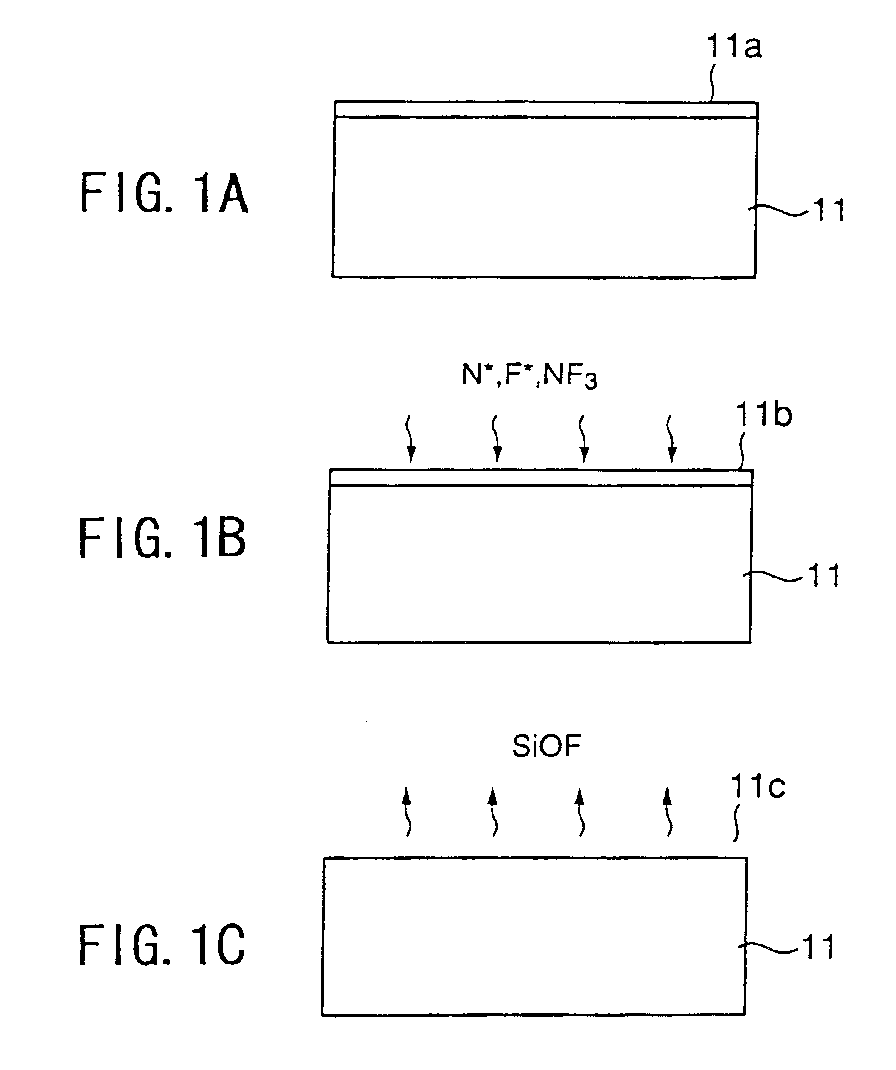
FIGS. 1A-1H show the process of forming a Ta2O5 film according to a first embodiment of the present invention.

Referring to FIG. 1A, a Si substrate 11 is held in a reaction vessel (not shown) under a reduced pressure environment of 133-399 Pa (1-3 Torr) at a temperature lower than a room temperature, and an oxide film 11a on the surface of the substrate 11 is removed by supplying nitrogen radicals N* and hydrogen radicals H* formed as a result of plasma activation of a gas mixture of N2 and H2 into the reaction vessel together with a NF3 gas. By conducting such a removal of the oxide film at low temperature, there is formed a protective film 11b having a composition of N—O—Si—H on the surface of the Si substrate 11. In a typical example, the H2 gas, the NF3 gas and the N2 gas are supplied with respective flow rates of 10 sccm, 30 sccm and 100 sccm, and the activation of the H2 gas and the N2 gas is achieved by applying a plasma power of about 50 W. The process of FI...

second embodiment

[Second Embodiment]

FIG. 7 shows the process of forming a dielectric film according to a second embodiment of the present invention in the form of flowchart.

Referring to FIG. 7, the gaseous molecules of SiCl4 are adsorbed on the SiO2 molecular layer 12a represented in FIG. 1D in the step S1, and the SiCl4 molecules thus adsorbed are subjected to an oxidation or hydrolysis reaction in the step S2. As a result, there is formed a molecular layer of SiO2 on the substrate 11.

The foregoing steps S1 and S2 are repeated alternately a predetermined times X in the next step S3, and the process proceeds further to the step S4 corresponding to the process steps of FIGS. 1E and 1F in which the molecules of ZrCl4 or Zr(t-OC4H9)4 are adsorbed on the SiO2 molecular layer formed in the previous steps S1 and S2.

The gaseous molecular compound of Zr thus adsorbed are then subjected to an oxidation or hydrolysis reaction in the next step S5 corresponding to the process step of FIG. 1G, and there is forme...

third embodiment

[Third Embodiment]

FIG. 9 shows the structure of a dielectric film according to a third embodiment of the present invention, wherein those parts corresponding to the parts described previously are designated by the same reference numerals and the description thereof will be omitted.

Referring to FIG. 9, the present embodiment carries out adsorption of SiCl4 molecules on the SiO2 molecular layer 12a and the SiCl4 molecules are converted to a molecular layer 12d of SiN by processing the adsorbed SiCl4 molecules by an NH3 gas. After the formation of the SiN molecular layer 12d, the Ta(OC2H5)5 molecules are adsorbed on the layer 12d, and are converted to the Ta2O5 molecular layer 12c as a result of oxidation. Further, the CVD-Ta2O5 layer 13 is formed on the Ta2O5 molecular layer 12c.

In the structure of FIG. 9, it is possible to eliminate the problem of diffusion of B into the Si substrate by the SiN molecular layer 12d when a B-doped polysilicon film is deposited on the Ta2O5 film 13. It...


PUM

PropertyMeasurementUnit
Dielectric polarization enthalpyaaaaaaaaaa
Concentrationaaaaaaaaaa

Abstract

A method of forming a dielectric film on a Si substrate comprises the steps of adsorbing a gaseous molecular compound of a metal element constituting a dielectric material on a Si substrate, and causing a decomposition of the gaseous molecular compound thus adsorbed by a hydrolysis process or pyrolytic decomposition process or an oxidation process.

Description

TECHNICAL FIELDThe present invention generally relates to semiconductor devices and more particularly to a fabrication process of ultrafine and ultrahigh-speed semiconductor devices.BACKGROUND ARTWith advancement in the art of device miniaturization, it is now becoming possible to use a gate length of 0.1 μm or less in leading-edge, ultrahigh-speed semiconductor devices. With increase in the degree of device miniaturization, it is well known that there occurs an increase of the operational speed. On the other hand, in order to achieve such an increase of operational speed by way of device miniaturization, there is a requirement, from scaling law, to reduce the thickness of a gate insulation film used therein in proportion with the reduction of a gate length of the semiconductor device.In the case of ultrafine and ultrahigh-speed semiconductor devices having the gate length of 0.1 μm or less, it is thus necessary to reduce the thickness of the gate electrode to 1-2 nm or less, provid...

Claims


Application Information

Patent Timeline
IPC IPC(8): C23C16/02C23C16/40H01L21/02H01L21/28H01L29/51H01L29/40H01L21/316C23C16/44C23C16/455H01L29/78
CPCC23C16/0218H01L29/517C23C16/0236C23C16/0272C23C16/401C23C16/403C23C16/405C23C16/45525H01L21/28185H01L21/28194H01L21/31604H01L29/513C23C16/0227H01L21/31683H01L28/56H01L21/02189H01L21/02183H01L21/02178H01L21/02181H01L21/02271H01L21/022H01L21/02238H01L21/02194H01L21/0228H01L21/02164H01L21/02148H01L29/518
Inventor KIRYU, HIDEKIAOYAMA, SHINTAROTAKAHASHI, TSUYOSHISHINRIKI, HIROSHI
Owner TOKYO ELECTRON LTD
Why Eureka
Try Eureka