
System and method for monitoring high-frequency circuits

a high-frequency circuit and monitoring system technology, applied in direction finders using radio waves, instruments, superconductor devices, etc., can solve the problems of low input level, loss often becomes a real problem, analog circuits handling small signals would encounter low input levels, etc., to achieve the effect of reducing the loss of additional monitoring circuits and small spa

Inactive Publication Date: 2005-02-22
FUJITSU LTD
View PDF9 Cites 13 Cited by
  • Summary
  • Abstract
  • Description
  • Claims
  • Application Information

AI Technical Summary

Benefits of technology

In view of the foregoing, it is an object of the present invention to provide a system and method for monitoring a high-frequency circuit which minimize the insertion loss of additional monitoring circuits, while requiring only a small space.

Problems solved by technology

Further, the circuit may be placed in an ultra-low temperature environment to increase the conductivity, while there are some problems that have to be solved before it is put into practical use.
Another important aspect of the monitoring system is the transmission loss that a high-frequency signal will experience when it passes through some additional circuits attached for the purpose of monitoring.
While the amount of loss may depend on what frequency range is used or how the circuit is configured, the presence of loss often becomes a real problem when the quality of signals is critical.
Also, analog circuits handling small signals would encounter a problem of low input levels when insertion loss is present.
In high-power analog circuits, the monitoring circuits waste their output power.
Further, a directional coupler with a large coupling factor often causes a problem of distortion or loss of input and output signals of the high-frequency circuit to which the coupler is attached.

Method used


Image

  • System and method for monitoring high-frequency circuits
  • System and method for monitoring high-frequency circuits
  • System and method for monitoring high-frequency circuits

Examples


Embodiment Construction

Preferred embodiments of the present invention will be described below with reference to the accompanying drawings, wherein like reference numerals refer to like elements throughout.

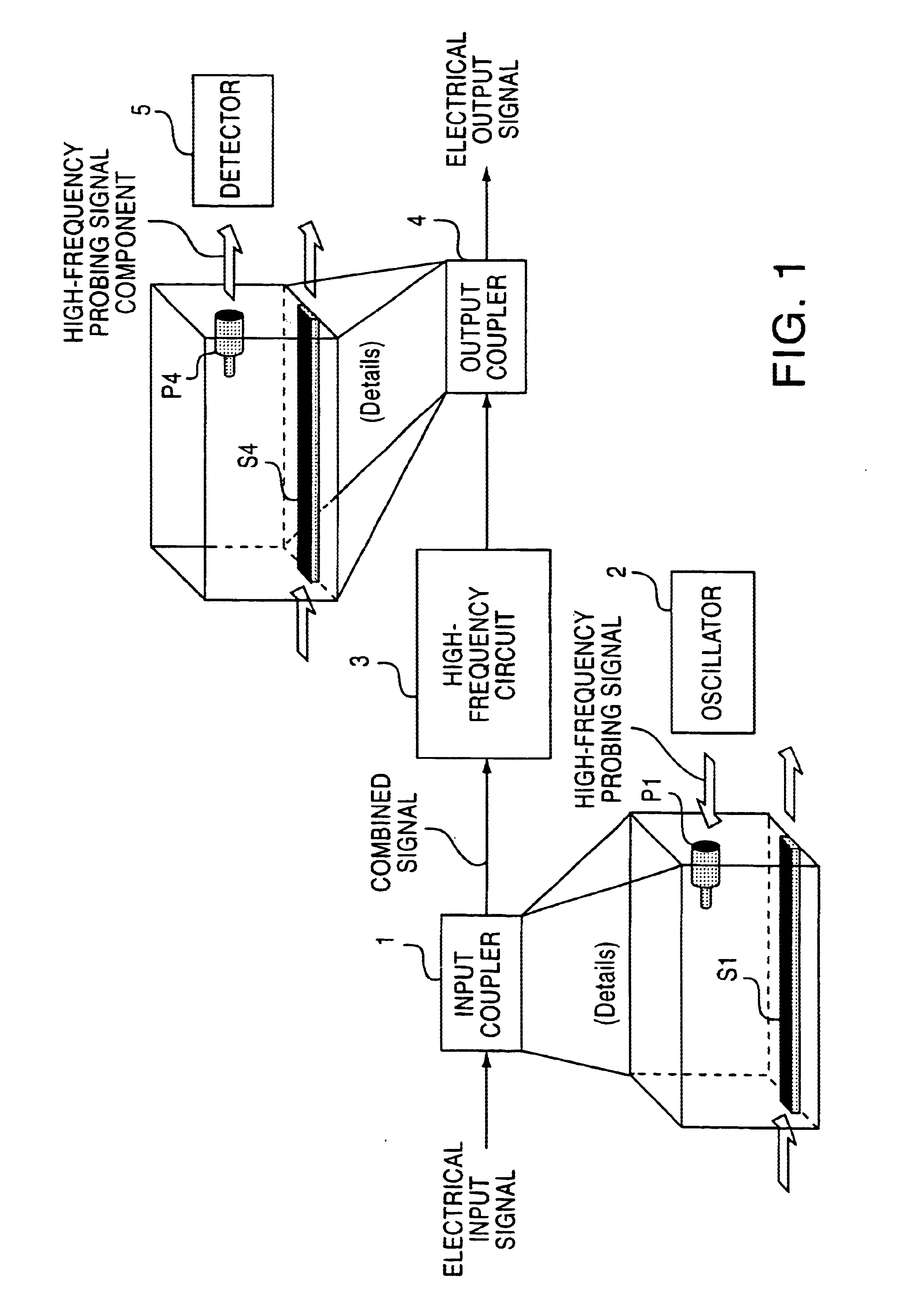
FIG. 1 is a conceptual view of a high-frequency circuit monitoring system according to the present invention. This monitoring system is applied to, for example, high-frequency circuits that are designed to operate at low temperatures to handle electrical signals in the spectral range of quasi-microwaves, microwaves, or millimeter waves. Note that the term “low temperatures” refers to cryogenic temperatures below the critical temperature of a superconductor (e.g., 80 K or lower).

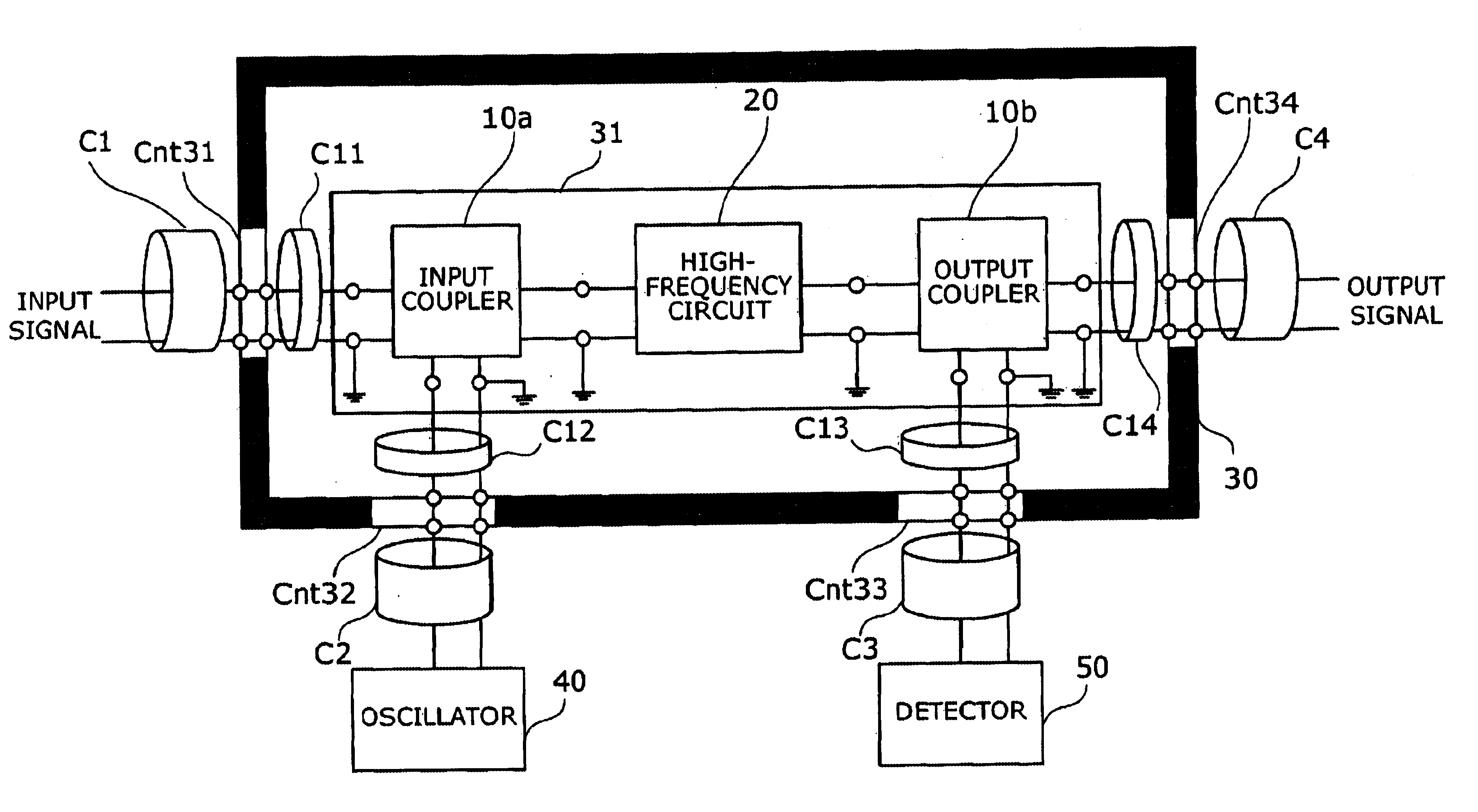
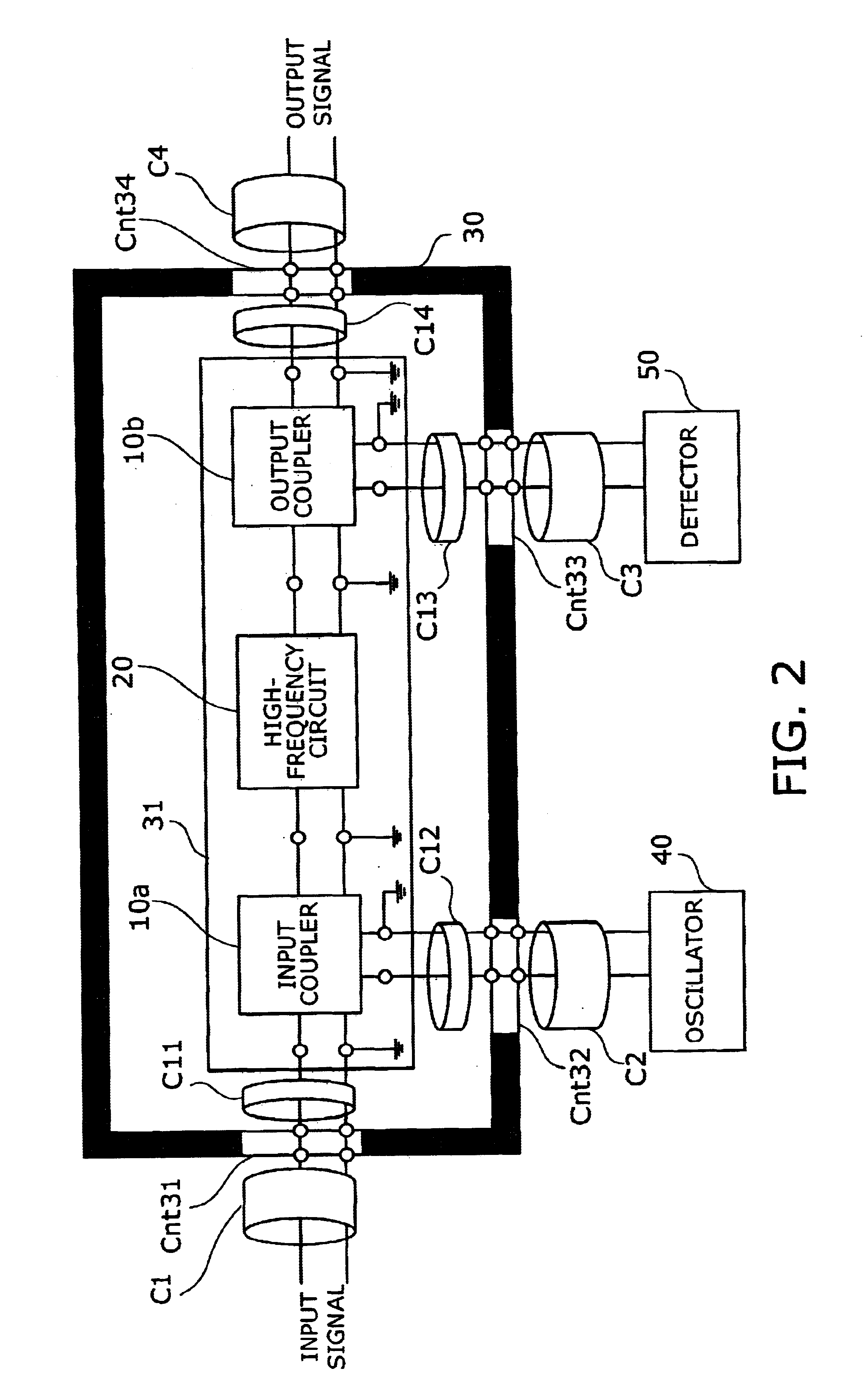
As can be seen in FIG. 1, the monitoring system comprises an input coupler 1, an oscillator 2, a high-frequency circuit 3, an output coupler 4, and a detector 5. Briefly, those elements function as follows. The oscillator 2 produces a high-frequency probing signal. The input coupler 1 combines this high-frequency probing signal wi...


PUM


Abstract

A monitoring system for high-frequency circuits which minimizes the insertion loss of additional monitoring circuits while requiring only a small space. An input coupler is placed at the input of a high-frequency circuit whose frequency response is to be monitored. The input coupler has a space where a given high-frequency probing signal can propagate, and it combines this propagating signal with a given electrical input signal. The combined signal is processed by the high-frequency circuit, and the resulting signal is supplied to an output coupler. The output coupler has a space for propagation of a high-frequency probing signal component contained in the received combined signal. The output coupler extracts this propagating signal component for the purpose of monitoring.

Description

CROSS-REFERENCE TO RELATED APPLICATIONSThis application is based upon and claims the benefit of priority from the prior Japanese Patent Application No. 2002-228121, filed on Aug. 6, 2002, the entire contents of which are incorporated herein by reference.BACKGROUND OF THE INVENTION1. Field of the InventionThe present invention relates to a system and method for monitoring a high-frequency circuit that operates at low temperatures to handle electrical signals in the spectral range of quasi-microwaves, microwaves, or millimeter waves. More particularly, the invention pertains to a monitoring system, as well as to a monitoring method therefor, that observes variations in the frequency response of a high-frequency circuit with minimum insertion loss.2. Description of the Related ArtRecent years have seen an increased demand for high-quality mobile network systems and satellite communications systems to meet the needs for wideband data transport of videos and images with better quality. T...

Claims


Application Information

Patent Timeline
Patent Type & Authority Patents(United States)
IPC IPC(8): H01P5/16H01P5/18H01P5/08
CPCH01P5/183
Inventor YAMANAKA, KAZUNORINAKAZAWA, ISAOSHIGAKI, MASAFUMIKAI, MANABU
Owner FUJITSU LTD
Learn More