Method of manufacturing and apparatus for a transmitter photonic integrated circuit (TXPIC) chip

a technology of integrated circuits and transmitters, applied in the field of photonic integrated circuits, can solve the problems of increased insertion loss, difficult fabrication, repeated basis, etc., and achieve the effects of reducing insertion loss at the modulator, reducing insertion loss, and improving chirp and extinction ratio

Inactive Publication Date: 2006-10-12
INFINERA CORP
View PDF36 Cites 11 Cited by
  • Summary
  • Abstract
  • Description
  • Claims
  • Application Information

AI Technical Summary

Benefits of technology

[0037] A TxPIC chip, as disclosed, comprises an array of modulated sources, preferably DFB lasers and optically coupled EA modulators, with the modulated outputs of the coupled to an integrated optical combiner, preferably an arrayed waveguide grating (AWG), from which the multiplexed output is presented at a facet output for optical coupling to an optical transport network or optical telecommunication system. The DFB lasers and EA modulators are optimized for highest output power, with improved chirp and extinction ratio as well as minimized insertion loss at the modulator, so that any need for on-chip signal amplification, such as a semiconductor optical amplifier (SOA), or a semiconductor optical laser amplifier or GC-SOA is eliminated.

Problems solved by technology

A principal reason is that it is difficult to fabricate, on a repeated basis, an array of DFB lasers with a wavelength grid that matches the wavelength grid of the AWG.
Also, as the numbers of electro-optic components are added to a PIC chip, insertion losses increase requiring that some on-chip or off-chip optical signal amplification is included.

Method used


Image

  • Method of manufacturing and apparatus for a transmitter photonic integrated circuit (TXPIC) chip
  • Method of manufacturing and apparatus for a transmitter photonic integrated circuit (TXPIC) chip
  • Method of manufacturing and apparatus for a transmitter photonic integrated circuit (TXPIC) chip

Examples


Embodiment Construction

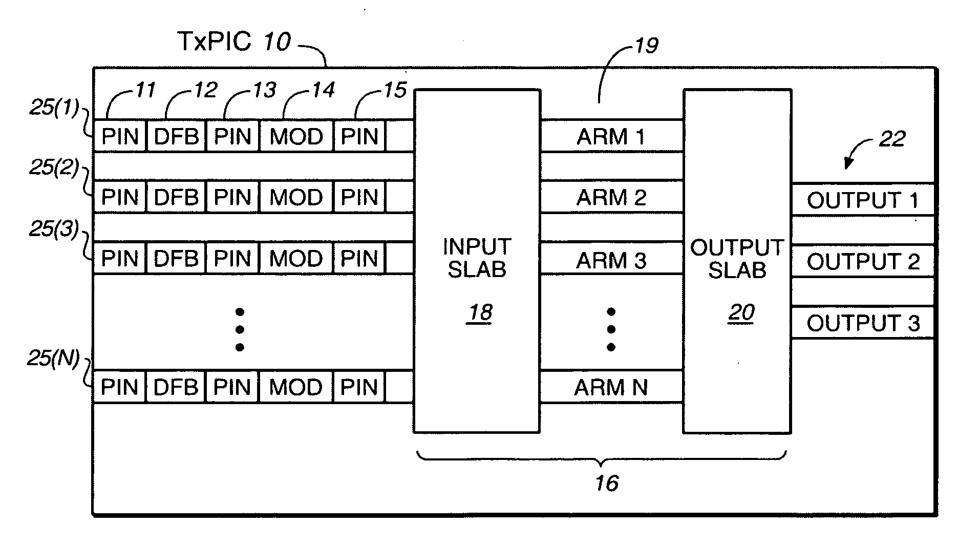
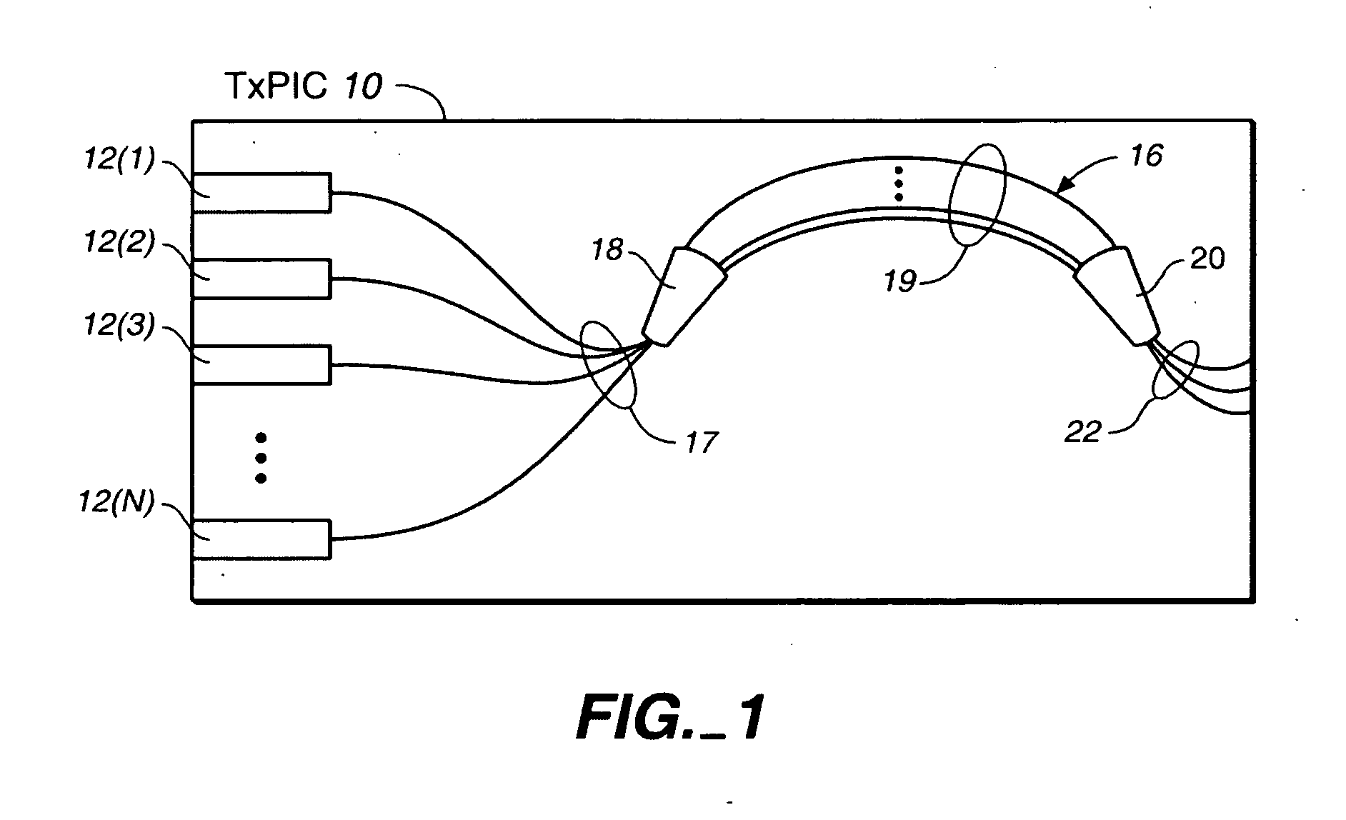
[0054] Reference is now made to FIG. 1 which discloses an InP-based semiconductor TxPIC 10 chip comprising, in monolithic form, a plurality of directly modulated DFB lasers 12(1) . . . 12(N) with their outputs 17 optically coupled to input slab 18 of to an optical combiner, shown here in the form of an arrayed waveguide grating (AWG) 16. AWG 16 comprises input slab or free space region 18 and output slab or free space region 20 between which are a plurality of waveguide gratings 19, all of which is known in the art. The output of AWG 16 is preferably a vernier output where more than one output 22 is provided from the center region of the first order Brillouin zone output of AWG 16. The vernier output 22, as indicated, is greater than one output, preferably equal to or greater than three different outputs, from output slab 20 of AWG 16 so that one of the outputs can be selected having an optimum AWG wavelength grid of aligned grid wavelengths. Thus, through the selection of the best ...


PUM


Abstract

A monolithic photonic integrated circuit (PIC) chip where the active waveguide cores of the modulated sources of the PIC are multiple quantum wells (MQWs) and the passive waveguide cores of an optical combiner are a bulk layer or material. The cores of the waveguide cores may be a quaternary such as InGaAsP or InAlGaAs.

Description

CROSS-REFERENCE TO RELATED APPLICATIONS [0001] This nonprovisional application is a continuation of patent application Ser. No. 10 / 267,346, filed Oct. 8, 2002 which claims the benefit of priority of provisional applications, Ser. No. 60 / 378,010, filed May 10, 2002 and entitled, TRANSMITTER PHOTONIC INTEGRATED CIRCUIT (TXPIC) CHIP WITH ENHANCED POWER AND YIELD WITHOUT ON-CHIP AMPLIFICATION; Ser. No. 60 / 328,207, filed Oct. 9, 2001 and entitled, PHOTONIC INTEGRATED CIRCUITS FOR DWDM OPTICAL NETWORKS, now U.S. nonprovisional patent application Ser. No. 10 / 267,331, filed Oct. 8, 2002 and entitled, TRANSMITTER PHOTONIC INTEGRATED CIRCUITS (TxPIC) AND OPTICAL TRANSPORT NETWORKS EMPLOYING TxPICs; Ser. No. 60 / 370,345, filed Apr. 5, 2002 and entitled, WAVELENGTH STABILIZATION IN TRANSMITTER PHOTONIC INTEGRATED CIRCUITS (TxPICs), now U.S. nonprovisional patent application Ser. No. 10 / 267,330, filed Oct. 8, 2002 and entitled, TRANSMITTER PHOTONIC INTEGRATED CIRCUIT (TxPIC) CHIP ARCHITECTURES AN...

Claims


Application Information

Patent Timeline
Patent Type & Authority Applications(United States)
IPC IPC(8): G02B6/12H01S5/026H01S5/0625H01S5/12H01S5/20H01S5/22H01S5/40
CPCG02B6/12019G02B6/12033H01S5/026H01S5/0265H01S5/06258H01S5/4031H01S5/12H01S5/204H01S5/205H01S5/22H01S5/106
Inventor JOYNER, CHARLES H.KISH, FRED A. JR.PETERS, FRANK H.MATHUR, ATULWELCH, DAVID F.DENTAI, ANDREW G.LAMBERT, DAMIENSCHNEIDER, RICHARD P.MISSEY, MARK J.
Owner INFINERA CORP
Why Eureka
Try Eureka