Thin film transistor formed on a resin substrate

Inactive Publication Date: 2005-02-08
SEMICON ENERGY LAB CO LTD
View PDF26 Cites 53 Cited by
  • Summary
  • Abstract
  • Description
  • Claims
  • Application Information

AI Technical Summary

Benefits of technology

The patterning mask of this patterning process is formed by exposing a positive photoresist to the light applied to the back of a transparent substrate and by developing it. The pattern made of the conductive film functions as a photolithography mask when the transparent substrate is exposed to the light applied to the back thereof and a photoresist pattern can be formed on the pattern made of the conductive film in a self-alignment manner. The photoresist pattern narrower than the pattern made of the conductive film can be formed with good accuracy by controlling an exposure time and a developing time.
According to the present invention, the length of the low-concentration impurity region is determined by the photoresist pattern like the conventional method, but the photoresist pattern in accordance with the present invention is formed in a self-alignment manner by exposing the substrate to the light applied to the back thereof and the width of the photoresist pattern can be formed with high accuracy by controlling the exposing time and the developing time. Therefore, even if a thin film transistor is made finer and a substrate is increased in area, the length of the low-concentration impurity region can be controlled with high accuracy and with good reproducibility. Further, since the number of photolithography masks can be omitted by one, costs can be reduced and the number of mask alignment processes is reduced and throughput can be expected to improve.

Problems solved by technology

However, in the TFT using the polycrystalline silicon, a current leaking from a drain in an off state (that is, off current) is large, and hence, if it is used as the switching element of a matrix circuit, it can not hold the electric potential of the pixel electrode.
Therefore, it has been a big problem to reduce the off current of the TFT.
Therefore, in order to form the low-concentration impurity region with high accuracy, a photolithography mask is required to be aligned with high accuracy, but there is a problem that as an element becomes finer and a liquid crystal panel becomes larger in area, an alignment accuracy becomes lower.
In the above Japanese Patent, a photoresist is not used as the doping mask and hence the length of the low-concentration impurities region can be controlled with high accuracy, but there is a drawback that the gate electrode material is limited to aluminum.
Also, there is another problem that the process temperature is limited to about 400° C. after an aluminum wiring is formed and that aluminum atoms are diffused into a gate insulating film to easily make a short circuit between a gate wiring and a channel, thereby reducing reliability.
Therefore, it is necessary to arrange a circuit in consideration of the process margin of etching, which prevents a high-integration design.

Method used


Image

  • Thin film transistor formed on a resin substrate
  • Thin film transistor formed on a resin substrate
  • Thin film transistor formed on a resin substrate

Examples


embodiment 1

[Preferred Embodiment 1]

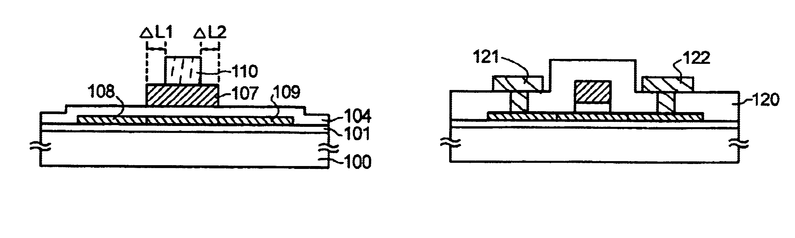
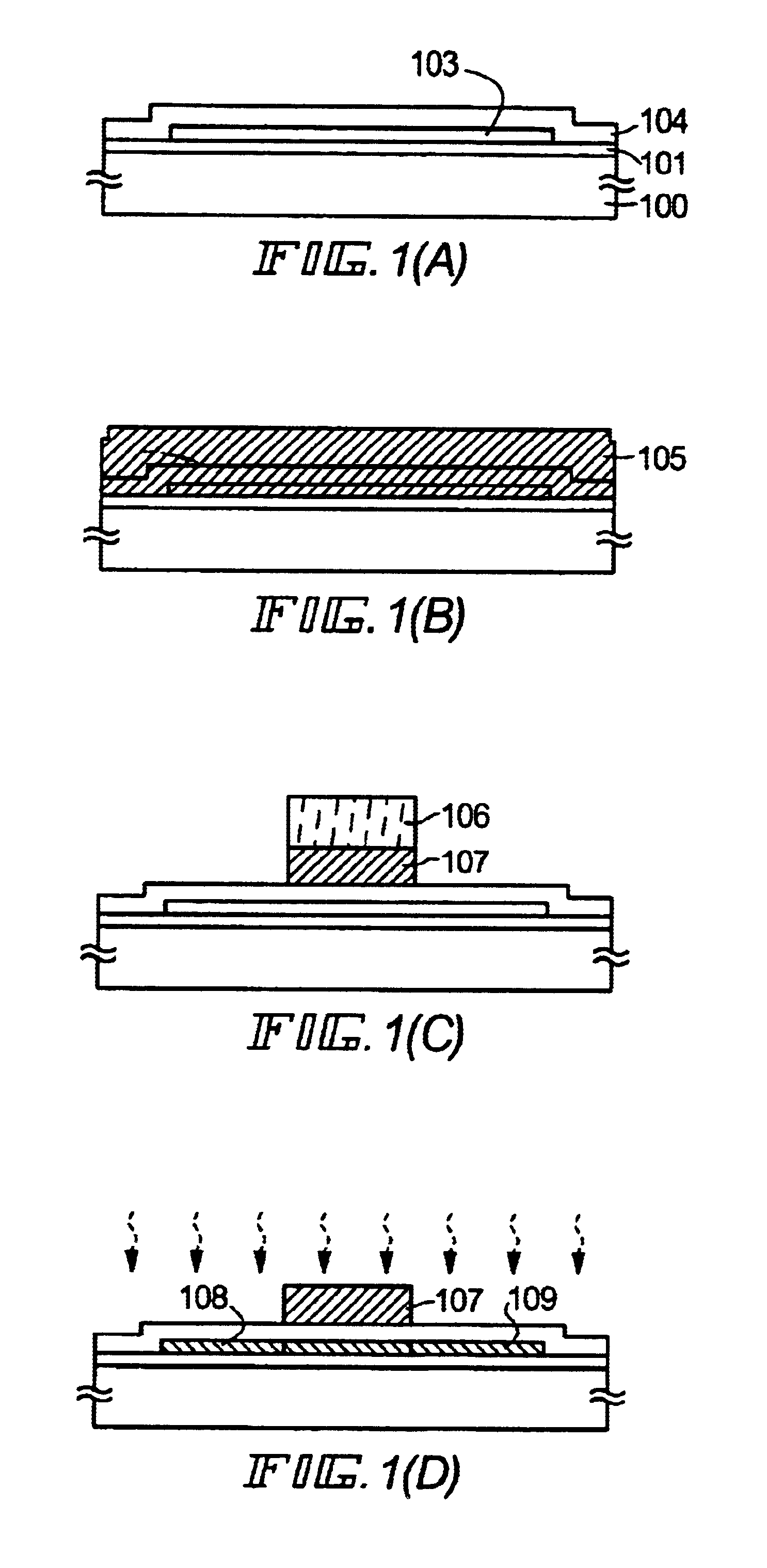
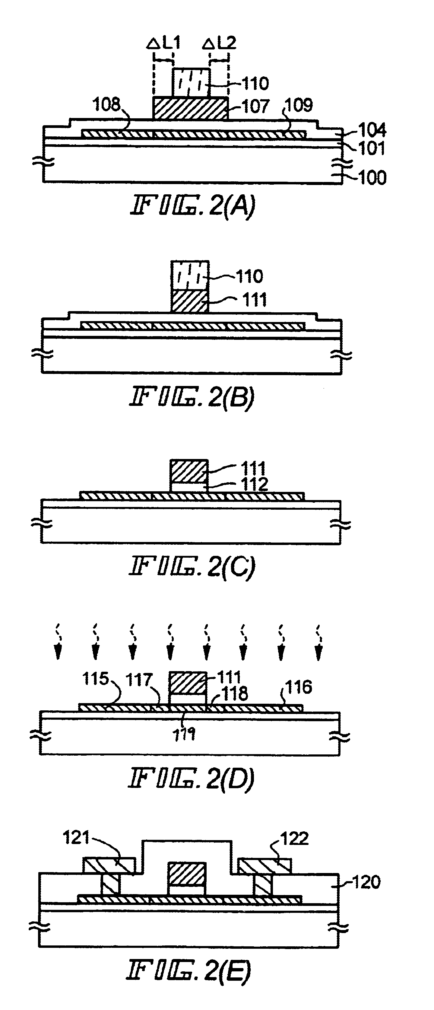
The present preferred embodiment relates to a manufacturing method of a TFT having an LDD structure. FIG. 1 and FIG. 2 are cross-sectional views showing a manufacturing process and cross-sectional views in the direction of length of the channel of the TFT.

First, an underlayer film 101 is formed on the whole surface of a substrate 100, and an island-shaped semiconductor layer 103 is formed on the underlayer film 101. An insulating film 104 to be a gate insulating film and covering the semiconductor layer 103 is formed on the whole surface of the substrate 100 (see FIG. 1(A)).

A transparent substrate having a transmissivity of 80% or more, more preferably, of 90% or more, to light applied to the back of the substrate (coherent light having a wavelength 400 nm or less), which is described below, is used as the substrate 100. For example, a glass substrate, a quartz substrate, a crystalline glass substrate, and a resin substrate such as a polyethylene terephthalat...

embodiment 2

[Preferred Embodiment 2]

In the preferred embodiment 1, a method of manufacturing a TFT having an LDD structure has been described, and in this preferred embodiment, a method of manufacturing a TFT having an offset structure will be described. The present preferred embodiment will be described by using FIGS. 1 and 2.

In the case of the present preferred embodiment, the impurity adding process shown in FIG. 2(D) is omitted, and in the impurity adding process shown in FIG. 1(D), a high concentration doping is performed at a dose of 1×10¹⁵ / cm2 to 1×10¹⁷ / cm2 so that the concentration of phosphorus becomes 1×10¹⁹ atoms / cm3 to 1×10²¹ atoms / cm3, thereby sufficiently reducing sheet resistance. As a result, a TFT can be manufactured in which the regions 117, 118 become offset regions.

example 1

The present example is the one applied to a CMOS circuit. The manufacturing process of the CMOS circuit of the present example will be described with reference to FIG. 3 and FIG. 4. FIGS. 3 and 4 are cross-sectional views along the direction of length of the channel of the TFT.

A glass substrate 200 is prepared. In the present example, a 1737 glass substrate made by Corning Glass Corp. is used. An underlayer film 201 is formed on the surface of the glass substrate 200. A silicon oxide film having a thickness of 200 nm is formed by plasma CVD by using TEOS (tetra ethoxy silane) gas as a raw material. The underlayer film 201 is heated at 400° C. for 4 hours.

An amorphous silicon film having a thickness of 500 nm is formed on the underlayer film 201 by plasma enhanced CVD (hereinafter referred to as PECVD) by the use of SiH4 diluted with an H2 gas. A low pressure CVD may be used instead of the PECVD. The amorphous silicon film is heated and dehydrogenated at 450° C. for one hour, whereby...


PUM


Abstract

The object of the present invention is to form a low-concentration impurity region with good accuracy in a top gate type TFT. Phosphorus is added to a semiconductor layer by using a pattern made of a conductive film as a mask to form an N-type impurity region in a self-alignment manner. A positive photoresist is applied to a substrate so as to cover the pattern and then is exposed to light applied to the back of the substrate and then is developed, whereby a photoresist 110 is formed. The pattern is etched by using the photoresist pattern as an etching mask to form a gate electrode. A channel forming region, a source region, a drain region, and low-concentration impurity regions, are formed in the semiconductor layer in a self-alignment manner by using the gate electrode as a doping mask.

Description

BACKGROUND OF THE INVENTION1. Field of the InventionThe present invention relates to a method of manufacturing a thin film transistor and an active matrix substrate using the thin film transistor as a switching element.2. Description of the Related ArtsA thin film transistor (hereinafter referred to as a TFT) is utilized for the switching element of a pixel electrode of an active matrix type liquid crystal display device. As the demand for a high-definition liquid crystal display grows, the semiconductor layer of the TFT is required to be formed of polycrystalline silicon instead of amorphous silicon.If the semiconductor layer of a TFT is formed of polycrystalline silicon, it is possible to manufacture the TFT such that it has high mobility and a large on-current, and hence not only a pixel matrix circuit but also a driver circuit can be integrally formed on the same substrate. However, in the TFT using the polycrystalline silicon, a current leaking from a drain in an off state (tha...

Claims


Application Information

Patent Timeline
IPC IPC(8): H01L21/70H01L21/02H01L29/786H01L29/66H01L21/336H01L27/12H01L21/84G02B5/30G02B27/01H01L21/77H01L29/49
CPCG02B27/017G02B27/0172H01L27/124H01L29/4908H01L29/66757H01L29/78621H01L29/78627H01L33/16H01L27/12G02B5/30G02B2027/0178G02F2001/13625G09G3/3225G02F1/13625
Inventor OHTANI, HISASHI
Owner SEMICON ENERGY LAB CO LTD
Why Eureka
Try Eureka