
Semiconductor device

a technology of semiconductor integrated circuits and devices, applied in the direction of individual semiconductor device testing, semiconductor/solid-state device testing/measurement, instruments, etc., can solve the problems difficult to individually and reliably cut off the fuses, and the risk of malfunctioning of the semiconductor integrated circuit b>1/b>, so as to achieve the effect of increasing the testing tim

Inactive Publication Date: 2005-01-04
PANASONIC CORP
View PDF10 Cites 19 Cited by
  • Summary
  • Abstract
  • Description
  • Claims
  • Application Information

AI Technical Summary

Benefits of technology

It is an object of the present invention to provide a semiconductor device in which multiple testing pads can be arranged on a parting line, while avoiding malfunctions due to cutting of the testing pads and the testing circuit arranged on the a parting line, without requiring additional steps and increasing the testing time.
According to these configurations, it is possible to ensure that the internal circuit is prevented from being affected by the influence of a cutting plane when the testing pad or the testing circuit arranged on the parting line is cut off. Therefore, it is possible to arrange the multiple testing pads on the parting line, while additional steps beyond separating the semiconductor integrated circuit along the parting line, which have been performed conventionally, are not needed and the testing time is not increased.
According to this configuration, the mode of operation is fixed after separating the semiconductor integrated circuits along the parting line, so that malfunctions can be prevented. Furthermore, since it becomes impossible to input and output signals by using the testing pad, high security can be assured.

Problems solved by technology

However, in this case, there is a risk of malfunctioning of the semiconductor integrated circuit 1 because the cutting planes of the wires 8 may be short-circuited with a power supply, a ground power supply or any of the other signal lines when the semiconductor integrated circuits 1 are cut apart along the parting lines 2.
However, it is difficult to individually and reliably cut off the fuses 9 provided in the wires 8 that are connected to all of the testing pads 7 arranged on the parting lines 2.
Furthermore, an additional processing step of cutting off the respective fuses 9 is needed, which increases the testing time.

Method used


Image

  • Semiconductor device
  • Semiconductor device
  • Semiconductor device

Examples


embodiment 1

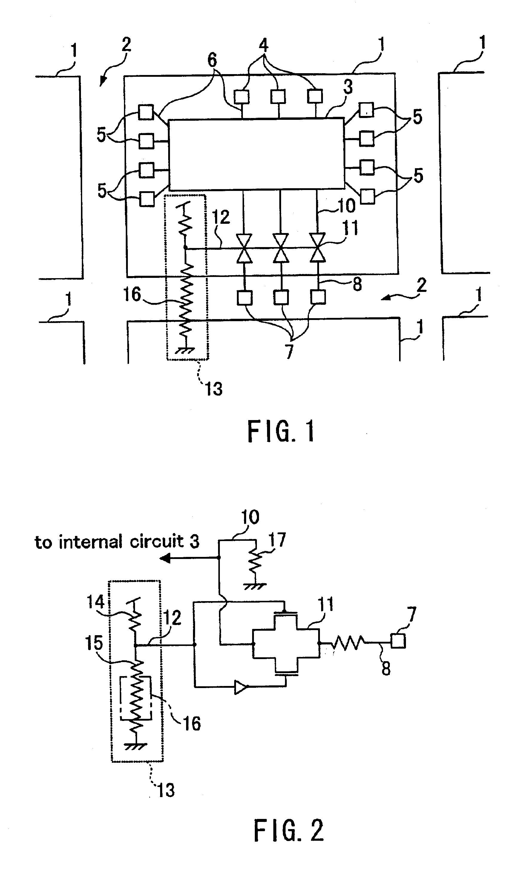
FIG. 1 shows a semiconductor device according to Embodiment 1 of the present invention. This semiconductor device includes a plurality of semiconductor integrated circuits 1 and parting lines 2 formed on a semiconductor wafer. Testing pads 4 and bonding pads 5 are arranged in order to input and output signals between an internal circuit 3 formed in the semiconductor integrated circuit 1 and the outside, and connected to the internal circuit 3 via wires 6. In addition, testing pads 7 to be used only during test are arranged on the parting lines 2 and connected to the internal circuit 3 via wires 8, wires 10 and switches 11. The testing pads 7 are cut away when the plurality of semiconductor integrated circuits 1 are separated from each other by cutting along the parting lines 2.

The switches 11 are elements connecting and disconnecting the internal circuit 3 and the testing pads 7. Before the semiconductor integrated circuit 1 is cut apart along the parting lines 2 and separated, the ...

embodiment 2

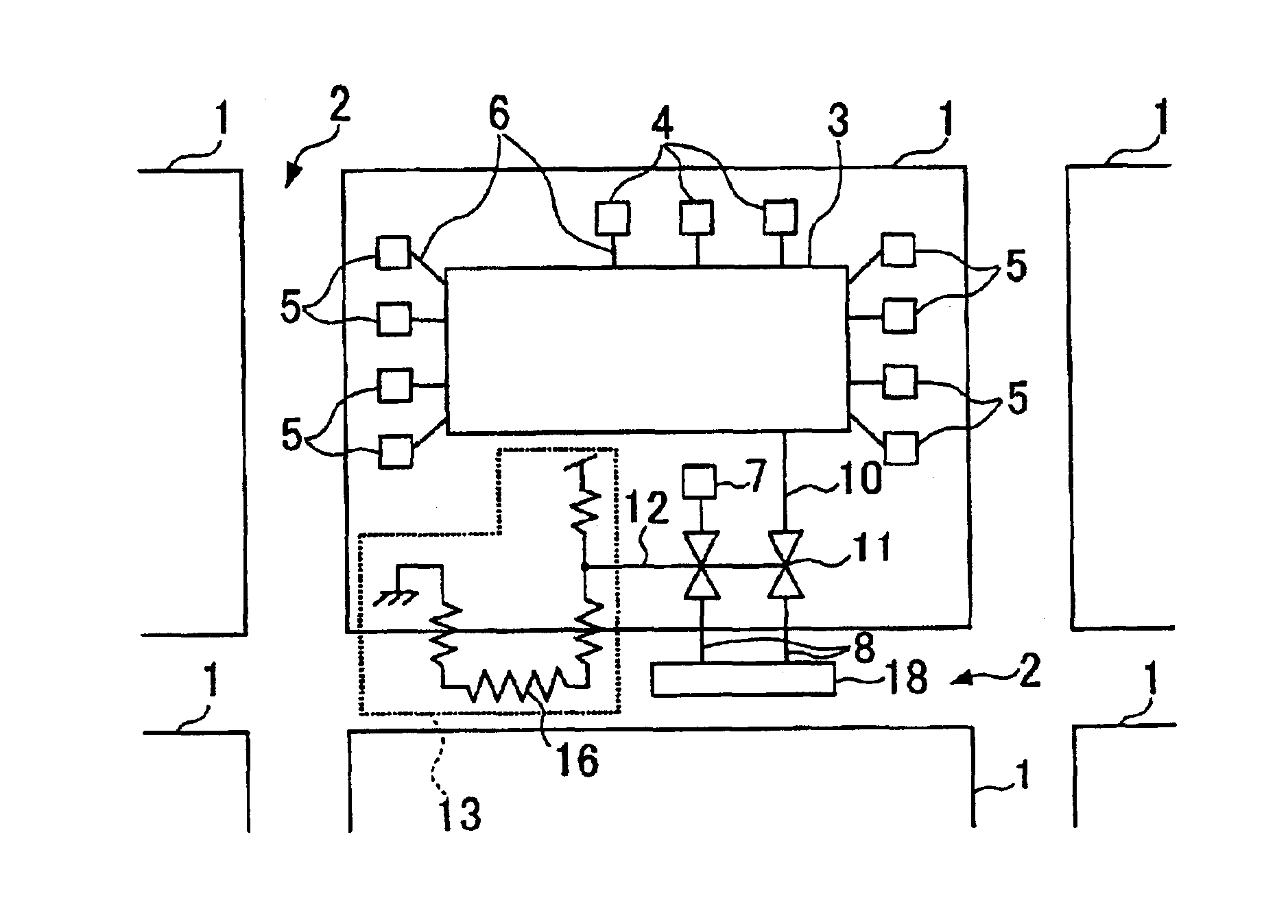
FIG. 3 shows a semiconductor device according to Embodiment 2. In this semiconductor device, the area of the semiconductor integrated circuit 1 is reduced by arranging an testing circuit 18, which used to be arranged within the semiconductor integrated circuit 1, on the parting line 2. Also in this case, the switches 11 are arranged between the wires 8 and the wires 10 that connect the testing circuit 18 to the internal circuit 3. The switches 11 are turned on and off by the switching element 13 connected via the wire 12. The switching element 13 has a resistive element 16 arranged on the parting line 2. Accordingly, even when the testing circuit 18 is cut away during the separation along the parting line 2 and the cutting plane of the wire 8 is short-circuited with the ground power supply VSS, the power supply VDD or any of the other signal lines, it is possible to prevent the internal circuit 3 from being affected, because the resistive element 16 is cut off simultaneously and the...

embodiment 3

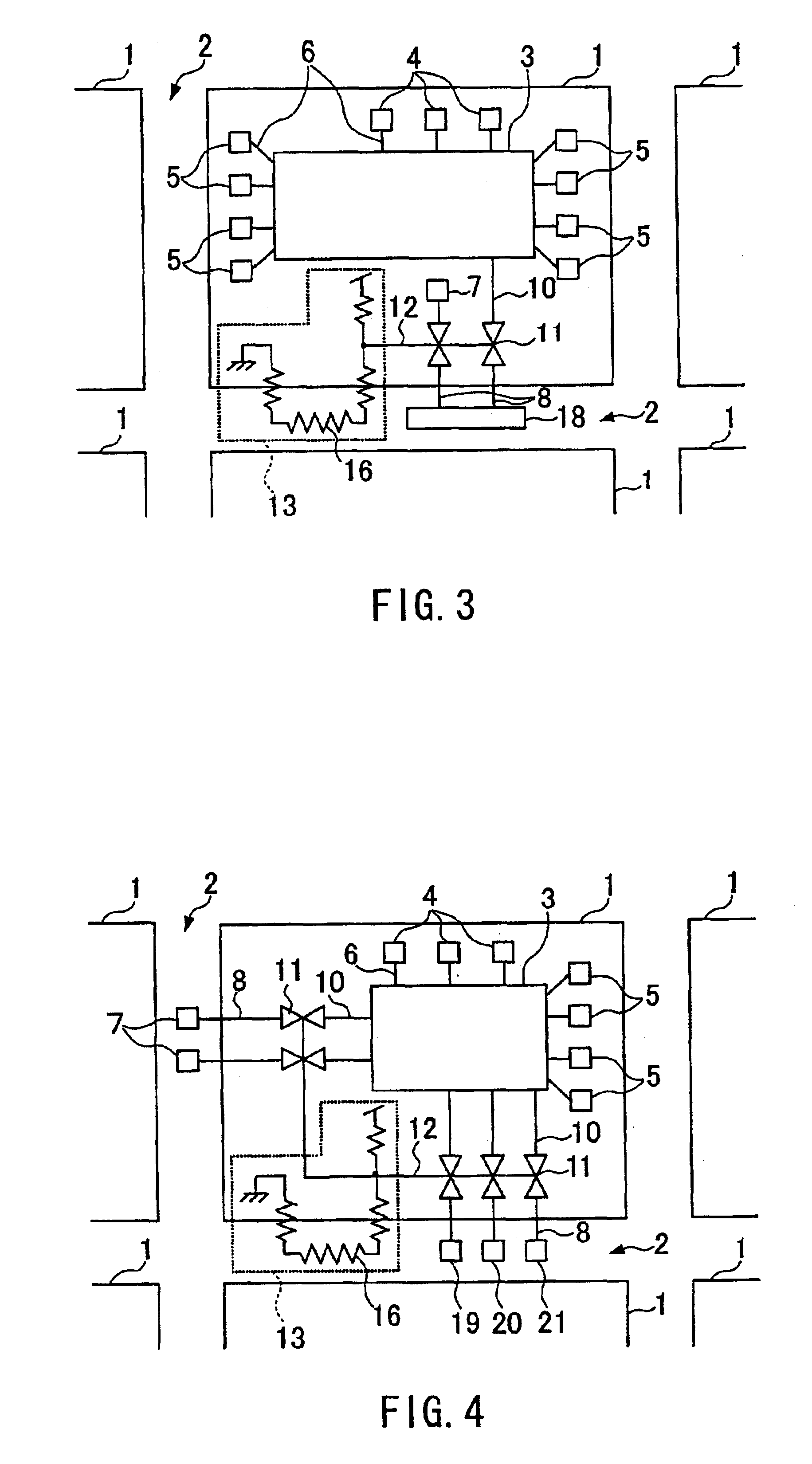
FIG. 4 shows a semiconductor device according to Embodiment 3. In this semiconductor device, the area of the semiconductor integrated circuit 1 is reduced by arranging pads 19, 20 and 21 for selecting the operation mode of the semiconductor integrated circuit 1 on the parting line 2.

The mode of operation of the semiconductor integrated circuit 1 can be changed by inputting and outputting signals to and from the operation mode selector pads 19, 20 and 21 at a predetermined timing. For example, in one mode of operation, it is possible to test memory, so that it becomes possible to read and write memory data by using the testing pad 4, the testing pad 7 or the like. Alternatively, in another mode of operation, it is possible to test digital circuit characteristics, so that it becomes possible to input and output data regarding the digital circuit characteristics by using the testing pad 4, the testing pad 7 or the like. Examples of means for changing these modes of operation are as fol...


PUM


Abstract

A semiconductor device includes a plurality of semiconductor integrated circuits formed on a semiconductor wafer; an testing pad for inputting and outputting a signal to and from an internal circuit of the semiconductor integrated circuit; a switch for switching a state of a connection between the semiconductor integrated circuit and the testing pad; and a wiring pattern formed on a parting line around the semiconductor integrated circuit and connected to an input terminal of the switch. When the semiconductor integrated circuits are separated, cutting off of the wiring pattern causes the switch to be turned off, so that the internal circuit is prevented from being affected by the influence of the cutting plane.

Description

FIELD OF THE INVENTIONThe present invention relates to a semiconductor device, in particular, to a semiconductor device provided with testing pads for inputting and outputting signals to and from an internal circuit of a semiconductor integrated circuit during testing, which are formed on a semiconductor wafer.BACKGROUND OF THE INVENTIONFIG. 6 is a partial plan view showing a conventional semiconductor device in which a plurality of semiconductor integrated circuits are formed on a semiconductor wafer. The plurality of semiconductor integrated circuits 1 are arranged on the semiconductor wafer and parting lines 2 are formed between the semiconductor integrated circuits 1. In order to input and output signals between an internal circuit 3 formed in the semiconductor integrated circuit 1 and the outside, testing pads 4 to be used during test and bonding pads 5 to be used after packaging of a product after the test are connected to the internal circuit 3 via wires 6.On the other hand, ...

Claims


Application Information

Patent Timeline
Patent Type & Authority Patents(United States)
IPC IPC(8): G01R31/28H01L23/58G01R31/3185H01L21/66H01L21/822H01L27/04
CPCG01R31/2884H01L22/32H01L2224/05554H01L2924/0002H01L2924/00
Inventor OHYA, MITSUYOSHINAKANE, GEORGE
Owner PANASONIC CORP
Learn More