The present invention exploits use of
tape casting to produce vacuum tight composite structures particularly useful for vacuum electronic device housings. In particular, the housing is formed from a laminate of
tape casting layers, and a cavity of desired volume is achieved by forming apertures in layers which are stacked upon a first end plate layer which latter directly or indirectly supports at least a portion of the electronic device.
Electrode leads are formed on selected pre-fired layers to communicate laterally through the walls of the cavity.
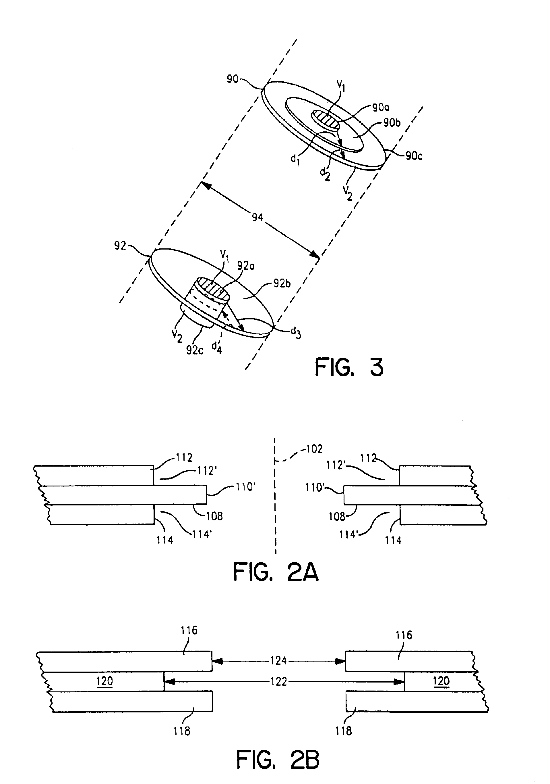
Electrical isolation is improved between selected regions of the cavity by varying the dimensions of substantially aligned apertures in non-monotonic fashion to produce an inwardly directed limiting aperture, or alternatively, an outwardly directed cavity extension, or channel. Improved
electrical isolation is thus obtained by extending the
linear distance on insulating surfaces between ground and
high potential, without increasing the external dimensions of the housing. The laterally directed electrical leads also allow for a more axially compact device and permit a vacuum electronic device to conform to form factors commonly applied to
semiconductor devices. Inwardly directed structures, separated by a layer of greater outward dimensions, produces a channel. In particular, the channel may be disposed close to a compressive seal and there arranged to capture the extruded flow of a vacuum
sealant. The present invention achieves vacuum sealing through a cold, crushed
soft metal seal directly between a planar metallized
ceramic surface and a closure member.
In particular, the present invention more fully utilizes tape cast housings for vacuum microelectronic devices. A great virtue of the tape cast structure is the freedom of formation of the
structural geometry. Another is the monolithic nature of the post-fired structure which permits deposit of
refractory metal conductive films between component layers thereby achieving electrical communication through a vacuum
enclosure without need for
insertion of separate
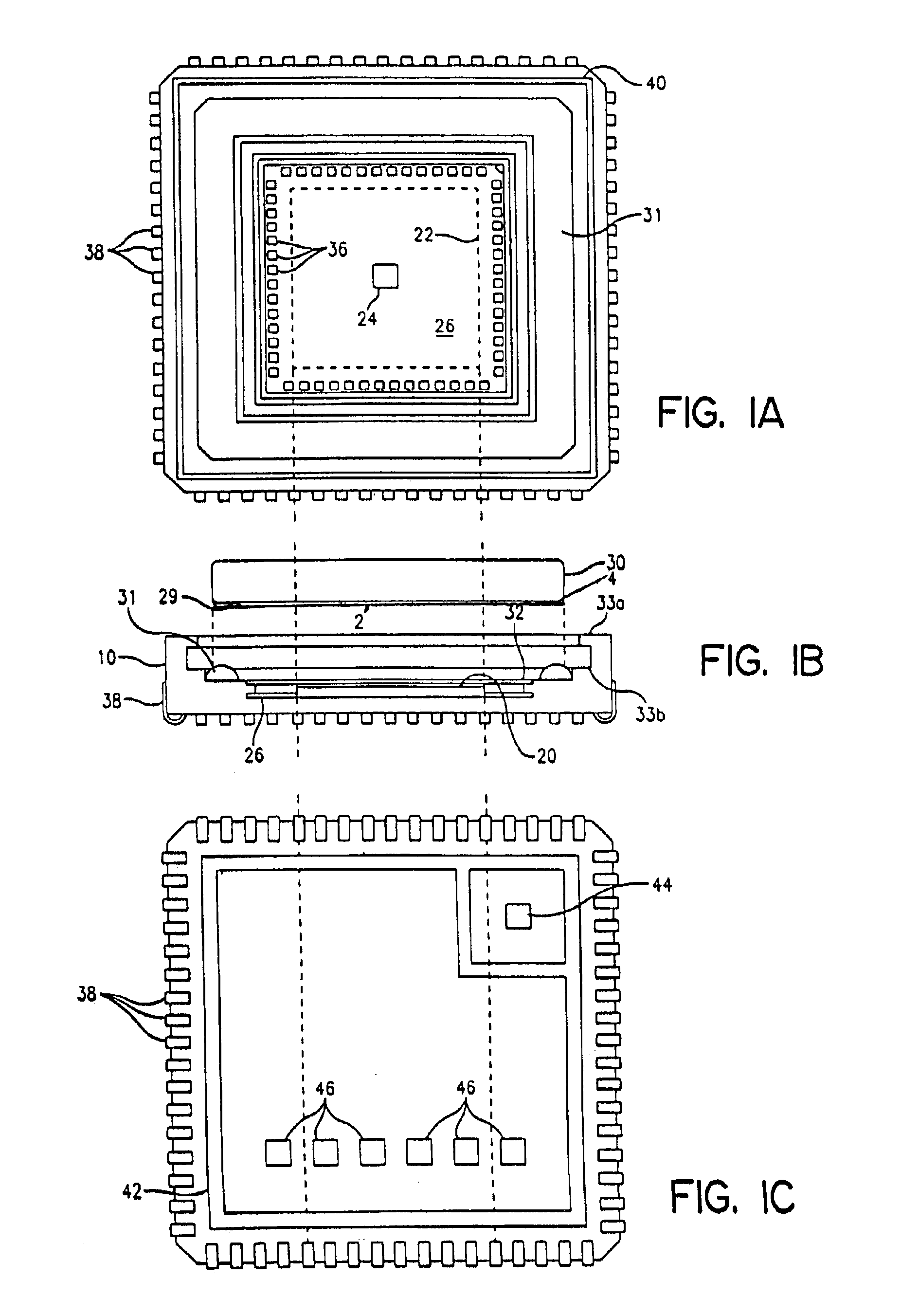
feedthrough terminals. Both of these features furnish subtle support for greater efficiencies in resulting vacuum electronic devices. For example, tape cast housings of the present invention are constructed to form internal cavities of generally rectangular cross section which match the generally rectangular form of typical components such as
semiconductor circuits or circuit elements realized on
semiconductor chips. In the present work, the specific example of an
image detector employs an array of diodes sensitive to increments of the
electron flux. Such arrays are commonly available in rectangular form. Matching the geometry of the component to the cavity permits a generally smaller cavity resulting in less wasted volume. The smaller
internal cavity implies the lesser internal surface area, which is favorable for the
ultra high vacuum (UHV) environment to be realized therein.
In like manner, forming conducting paths between the
green tape layers provides for distributing
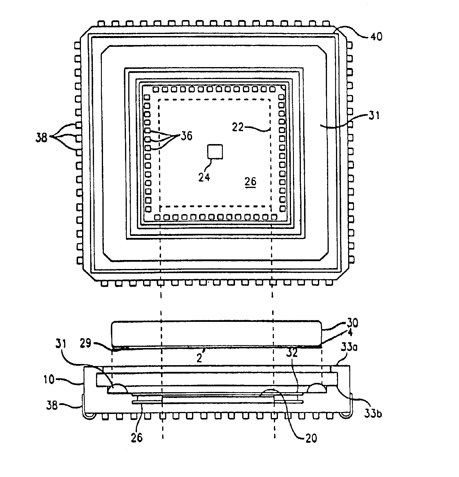
signal leads over the lateral walls of the housing in contrast to the practice of bringing all leads through the base of the structure. Accordingly, the inventive housing may be constructed to accommodate well known standards for integrated device sockets (JEDEC type PLCC open frame mounts). A further
advantage of laterally extending leads is that the resulting device can exhibit a more compact extension along its principal axis. In the exemplary
image detector device described herein, typical applications such as
night vision goggles can be formed for wear before the eyes with minimal inconvenience compared with comparable items of prior art.
Aside from the external advantages of a tape cast structure for microelectronic devices, there is an internal
advantage in forming consecutive layers having aperture dimensions which do not vary monotonically among a series of layers. Simply, the resulting cavity may be formed to have intruding wall portions adjacent to less intruding wall portions. These serrations can be utilized to provide for added
electrical isolation for relatively
high voltage conductors without increasing the external size of the
package. In like manner, a channel can be formed in the wall of the housing. Such channels are particularly useful adjacent to sealing medial where the compressed sealing media is allowed to flow into the channel for capture therein.
The vacuum microelectronic device is mounted within the tape cast housing and a closure member, including a sealing medium is installed and the seal effectuated in a vacuum environment at normal temperatures. Conventional vacuum preparation of the package includes a baking operation at about 300° C. to remove
outgassing sources and an
electron flux scrubbing to remove adsorbed residual gasses. For UHV microdevices a flat planar member is pressed against a flat metallized receiving surface of the
ceramic housing using a
soft metal (for example, In) interspersed therebetween and
mechanical pressure is applied to the closure member to effect a cold weld between the closure member and the receiving surface. An
adjacent channel proximate to the receiving surface receives the flow of the
sealant. Providing an edge
radius (or other window
peripheral detail) to this flat planar member,
proximate the
ceramic surface where the
soft metal extrudes, can improve the seal integrity.


