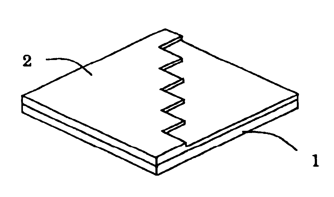
Echelon diffraction grating and optical waveguide element
a technology of diffraction grating and optical waveguide, which is applied in the direction of optical elements, optical waveguide light guides, instruments, etc., can solve the problems of film easily cracking, inferior heat resistance, and inability to apply the method to a diffraction grating having a lens function like a concave grating
- Summary
- Abstract
- Description
- Claims
- Application Information
AI Technical Summary
Benefits of technology
Problems solved by technology
Method used
Image

Examples
example 1
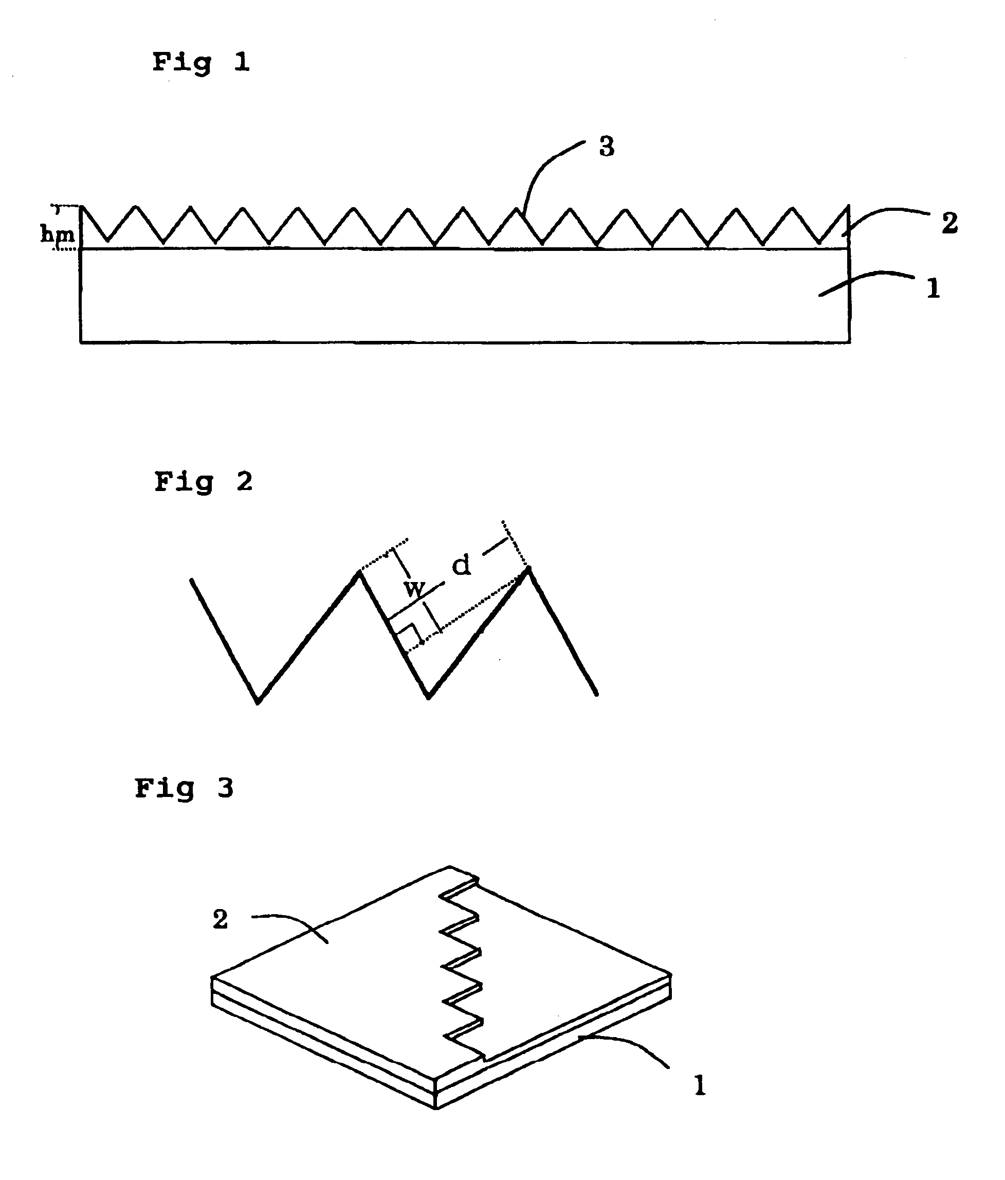
A 2.5 cm.times.2.5 cm soda-lime glass substrate having a thickness of 3.0 mm (linear expansion coefficient of 1.0.times.10.sup.-5 / .degree. C.) was subjected to ultrasonic alkali cleaning and further to pure water cleaning as a glass substrate. A 2.5 cm.times.2.5 cm silicon echelon diffraction grating having an average thickness of 2.0 mm (about 1,000 linear convex portions were formed on the surface of a silicon substrate by masking and etching, inclined surfaces on both sides of each convex portion agreed with a silicon crystal surface (1,1,1), the step height was 20.15 .mu.m and the step width was 14.3 .mu.m, the interval between adjacent grating lines (measured at ridges) was about 24.7 .mu.m, and the flat portion at top of each ridge (length of the remaining unetched portion) was about 5.0 .mu.m) was prepared as a mold. A fine uneven plate which was a reflection type echelon diffraction grating having a film thickness in a flat area (area devoid of the linear projection portion...
example 2
A 2.5 cm.times.2.5 cm silicon substrate having a thickness of 1.0 mm was subjected to ultrasonic alkali cleaning and further to pure water cleaning as a substrate. A 2.5 cm.times.2.5 cm aluminum plate having a thickness of 2.0 mm and a convex portion having a height of 10 .mu.m, a width of 10 .mu.m and a length of 20 mm was prepared as a mold. A plate having a concave portion as a clad portion was formed using the above substrate, mold and solution A in accordance with the substrate pouring process to ensure that the thickness of a film in the lowest area (portion in contact with the convex portion of the above mold) should become about 10 .mu.m. A heat treatment after coating was started at 160.degree. C. and the temperature was gradually raised to 180.degree. C. over 20 minutes and maintained at that temperature for 40 minutes. The pressing and heating conditions included a pressure of 2 kg / cm.sup.2, a temperature of 250.degree. C. and a time of 20 minutes. The mold was then relea...
example 3
An organopolysiloxane solution (solution C) was prepared in the same manner as the above solution (A) except that 0.1 mol of phenyltriethoxysilane and 0.175 mol of dimethyldiethoxysilane were used in place of 0.1 mol of phenyltriethoxysilane and 0.15 mol of dimethyldiethoxysilane.
A 2.5 cm.times.2.5 cm aluminum plate having a thickness of 2.0 mm and a groove as a concave portion having a depth of 2 .mu.m, a width of 2 .mu.m and a length of 20 mm was prepared as a mold. The mold was placed horizontal with the groove as a concave portion facing up, the above solution C was poured into the groove as a concave portion and heated at 150.degree. C. for 15 minutes, a 2.5 cm.times.2.5 cm quartz glass (refractive index of 1.460) substrate having a thickness of 1.0 mm was placed on the above mold, and the mold and the quartz glass substrate were inverted together. They were maintained at 200.degree. C. for 30 minutes while the molded film in the groove as a concave portion was contacted to the...
PUM
| Property | Measurement | Unit |
|---|---|---|
| Length | aaaaa | aaaaa |
| Wavelength | aaaaa | aaaaa |
| Wavelength | aaaaa | aaaaa |
Abstract
Description
Claims
Application Information
 - R&D
- Intellectual Property
- Life Sciences
- Materials
- Tech Scout
- Unparalleled Data Quality
- Higher Quality Content
- 60% Fewer Hallucinations
Browse by: Latest US Patents, China's latest patents, Technical Efficacy Thesaurus, Application Domain, Technology Topic, Popular Technical Reports.
© 2025 PatSnap. All rights reserved.Legal|Privacy policy|Modern Slavery Act Transparency Statement|Sitemap|About US| Contact US: help@patsnap.com