Electro-optic semiconductor devices and method for making the same

a semiconductor and optical technology, applied in the field of electro-optic semiconductor devices, can solve the problems of high input power requirements, high complexity and cost, and diffuse material can change the properties of the surrounding crystal growth layer,

Inactive Publication Date: 2003-10-07
HANGER SOLUTIONS LLC +1
View PDF4 Cites 6 Cited by
  • Summary
  • Abstract
  • Description
  • Claims
  • Application Information

AI Technical Summary

Benefits of technology

The term additive growth process is used to define a growth process in which a monolithic crystal structure is grown without any intermediate stages in which material is removed from the crystal previously grown. For example, it excludes growth processes which have an intermediate etching stage. Clearly, an additive growth process will generally be simpler and so will provide a cheaper way of making a monolithic crystal substrate comprising an active area located within a passive waveguide region.
The first part of the core of the waveguide is preferably selectively covered by a mechanical shadow mask which may be made of silicon coated with silicon oxide, silicon dioxide or silicon nitride in order to reduce the amount of crystal growth on the mask surface. To accurately define the edges of the active layer it is preferred that the edges of the shadow mask defining an aperture which exposes an area of the first part of the core of the waveguide are tapered so that the edges adjacent to the area of the first part of the core of the waveguide form the thin end of the taper.

Problems solved by technology

There are significant losses at interfaces between the separate component structures which lead to high input power requirements.
Also, problems of accurately optically aligning the separate component structures leads to high complexity and cost.
Unfortunately, the quantum well diffusion method only allows device to be grown within a passive waveguide.
Also, the diffuse material can change the properties of the surrounding crystal growth layers, for example, passive waveguide core layers, in an undesirable manner.
Also, this method of crystal growth requires a post processing quantum well intermixing step to destroy the selected areas of the layers of quantum wells, which adds expense.
The problem with this process is that the growth process has to be interrupted to perform at least one etching process.
This adds complexity and cost to the growth process and can reduce yield.
Also, the removal of the partly grown structure from the epitaxial growth chamber for the two etching stages and the processes involved in the etching stages can introduce contamination into the resulting device.
Accordingly, the method described is relatively complex and can have associated low yields.
Also, as the resulting device is monolithic there are very low coupling losses between the active area and the waveguide.

Method used


Image

  • Electro-optic semiconductor devices and method for making the same
  • Electro-optic semiconductor devices and method for making the same
  • Electro-optic semiconductor devices and method for making the same

Examples


Embodiment Construction

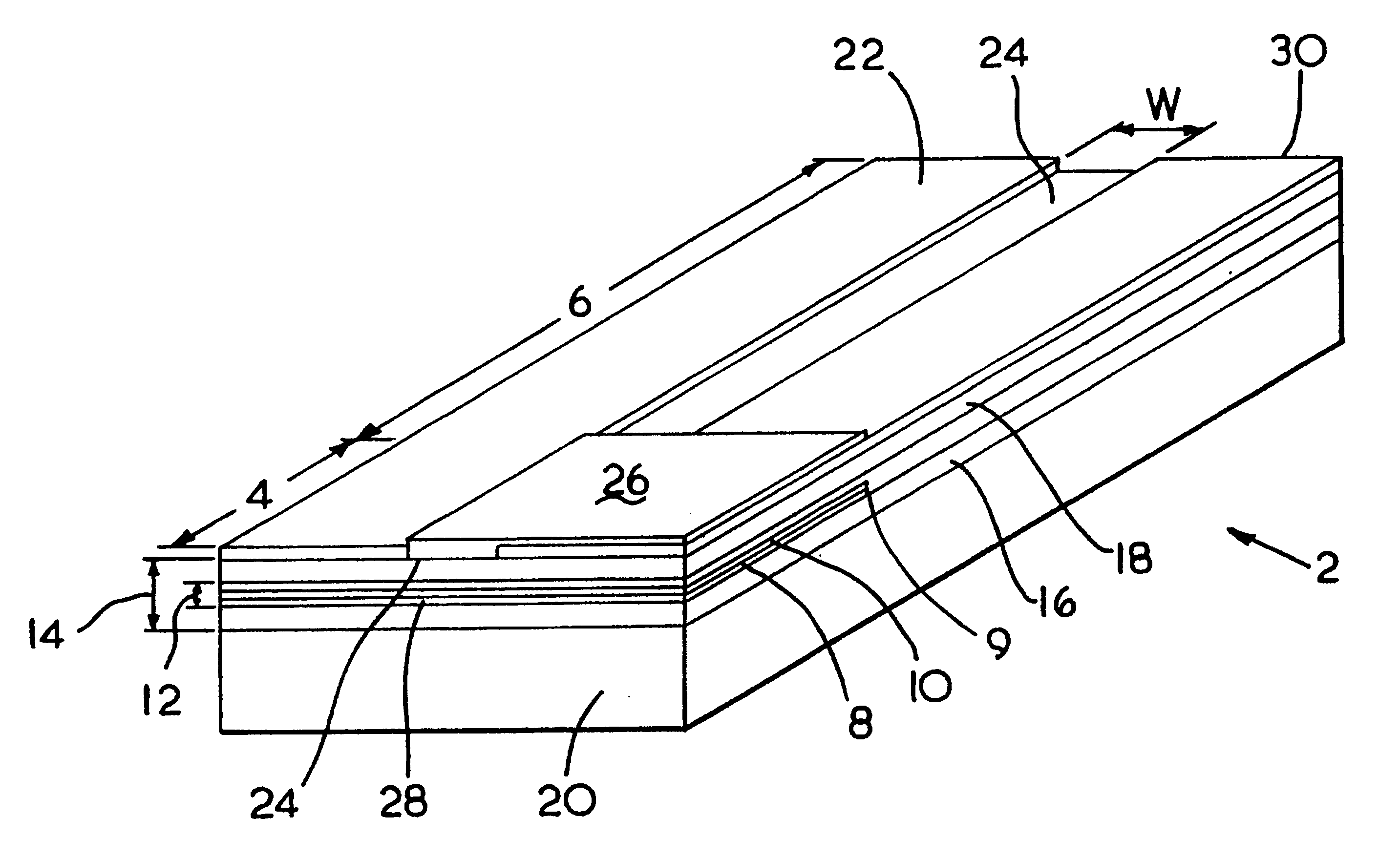
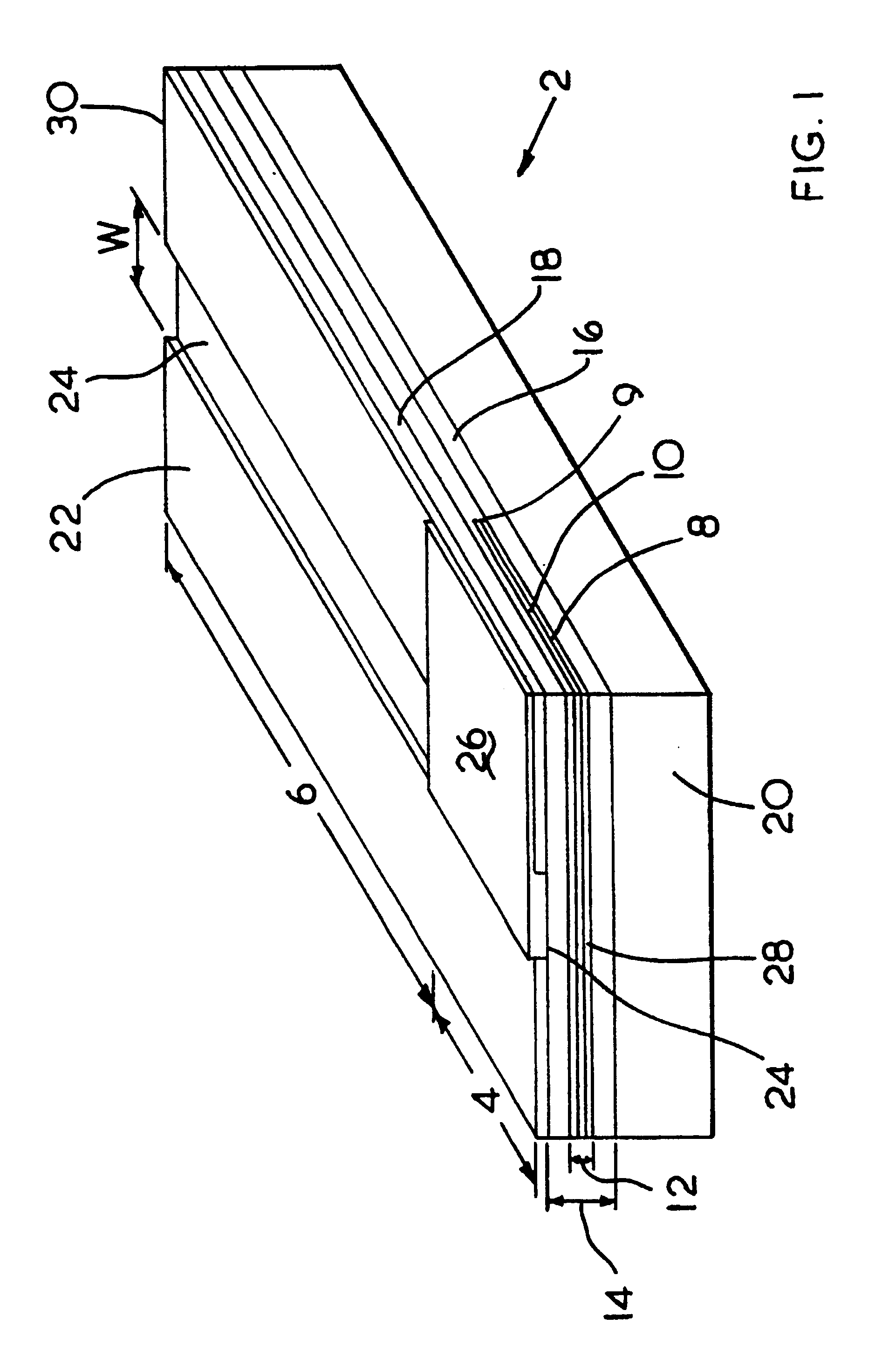
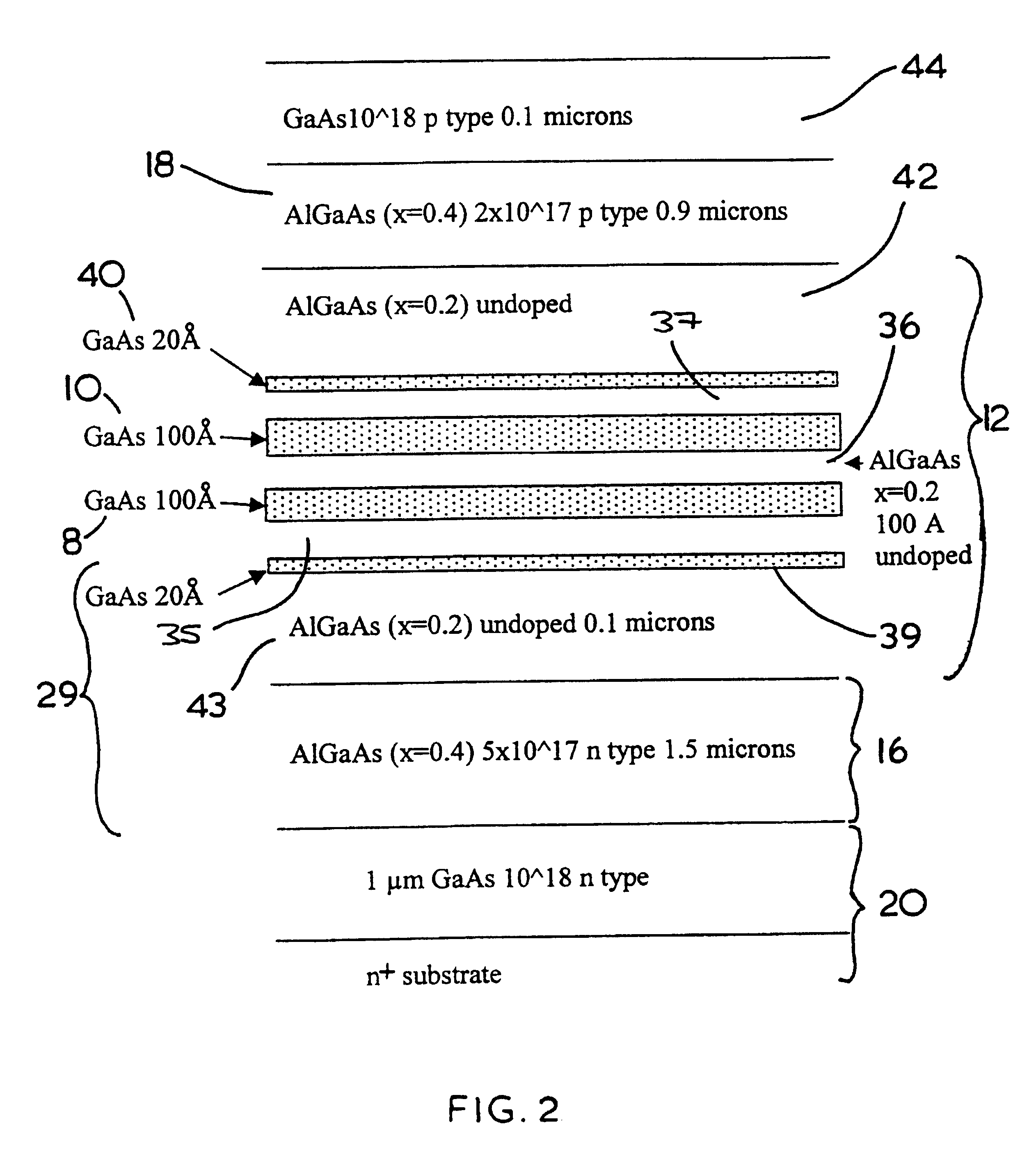
Referring first to FIG. 1, there is shown a monolithic extended cavity laser (2) comprising an active laser region (4) and a passive waveguide region (6). The active laser region (4) is formed by the selective growth of a two quantum well layers (8,10) in a core (12) of a waveguide (14). The two quantum well layers (8,10) form the narrow bandgap semiconductor material required for lasing action.

The quantum well layers (8,10) are each formed from a 100 A (100 Angstrom) thick layer of Gallium Arsenide (GaAs). The quantum well layers are grown within a layer of undoped Aluminium Gallium Arsenide (AlGaAs) comprising 20% Aluminium. The layer of 20% AlGaAs forms the core (12) of a waveguide (14) which extends through the active laser region (4) and passive waveguide region (6) of the extended cavity laser (2). The lower boundary or cladding layer (16) of the waveguide (14) is formed from a layer of n-type doped AlGaAs comprising 40% Aluminium which has a higher refractive index than the 2...


PUM


Abstract

An electro-optic semiconductor device comprising a semiconductor waveguide with a core region within which is located at least one active area wherein the core of the waveguide outside of the one or more active areas are not contaminated by diffuse active area material and the one or more active area(s) and the waveguide are monolithic and are grown in an additive growth process. Also provided is a method of making an electro-optic semiconductor device, comprising the steps of; growing a first part of a core layer of a semiconductor waveguide, selectively growing an active layer over a partial area of the first part of the core layer, and growing a second part of the core layer of the semiconductor waveguide over the first part and the active layer, characterised in that the method comprises an additive growth process.

Description

1. Field of the InventionThe present invention relates to electro-optic semiconductor devices which incorporate multiple active and passive component parts and methods for making the same. In particular the present invention relates to semiconductor lasers and detectors with integrated semiconductor waveguides and extended cavity semiconductor lasers and methods for making the same.2. Discussion of Prior ArtElectro-optic semiconductor devices are used in the quickly developing field of high speed analogue and digital optical signal processing circuitry which have applications in high speed, wide-bandwidth optomicrowave and optical transmission techniques particularly in the field of telecommunications.Electro-optic semiconductor components, such as semiconductor lasers and waveguides, are currently grown separately in different growth processes to generate different component structures on separate crystal substrates. Subsequently, the separate component structures are assembled int...

Claims


Application Information

Patent Timeline
IPC IPC(8): G02B6/12H01S5/00H01S5/026H01L27/15H01L31/12H01S5/343
CPCG02B6/12004H01S5/026G02B2006/12173H01S5/00
Inventor MARTIN, TREVORKANE, MICHAEL J
Owner HANGER SOLUTIONS LLC
Why Eureka
Try Eureka