
Flip chip and packaged memory module

Inactive Publication Date: 2002-11-05
CISCO TECH INC
View PDF18 Cites 51 Cited by
  • Summary
  • Abstract
  • Description
  • Claims
  • Application Information

AI Technical Summary

Problems solved by technology

The main drawback to using direct attach technology with MCMs including memory chips is the lack of reworkability of the memory chips, which tend to fail the most often.
If one of the memory chips fails during testing then the entire module, including the costly ASICs, CPUs, DSPs or other high value devices, must be scrapped since the epoxy filler material cannot easily be removed due to the epoxy underfill.

Method used


Image

  • Flip chip and packaged memory module
  • Flip chip and packaged memory module
  • Flip chip and packaged memory module

Examples


Embodiment Construction

Those of ordinary skill in the art will realize that the following description of the present invention is illustrative only and not in any way limiting. Other embodiments of the invention will readily suggest themselves to such skilled persons having the benefit of this disclosure.

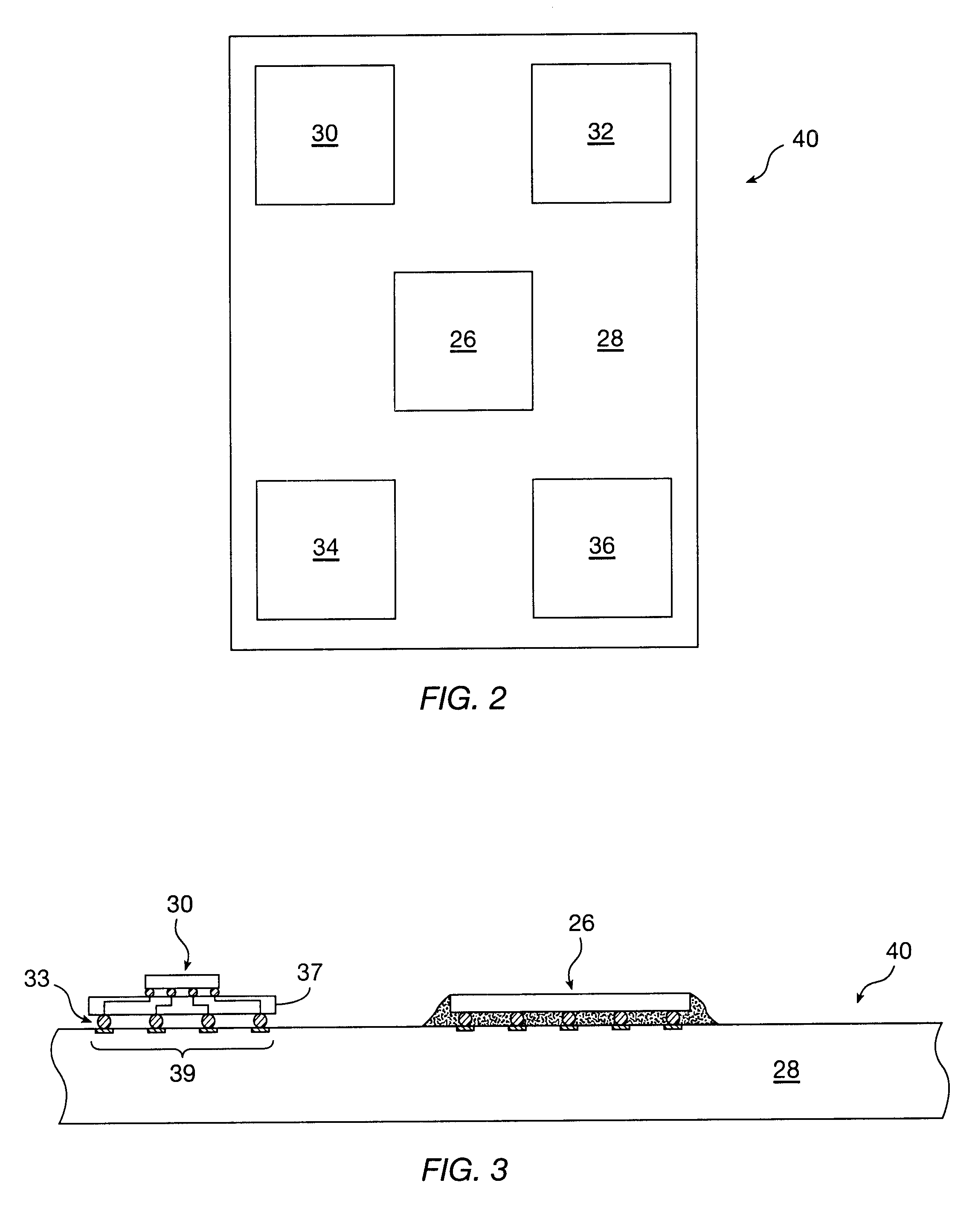
Turning now to FIG. 2, a top plan view of a MCM in accordance with a specific embodiment of the present invention is shown. One or more high value chips 26 such as ASICs, CPUs, DSPs or the like may be located at a position on MCM substrate 28. One or more memory chip packages 30, 32, 34, 36 are also located on MCM substrate 28. High value chip 26 has a large number of electrical connections to make with substrate 28 and is directly attached thereto using flip chip technology with an under fill of, for example, heat curable epoxy. As a result, high value chip 26 cannot be easily removed from substrate 28 once the underfill has cured.

Packaged memory chips 30, 32, 34, 36 are attached using a different attach...


PUM


Abstract

A multi-chip, module (MCM) having one or more high value chips such as ASICs, CPUs, DSPs or the like attached to the MCM substrate via a direct attach technology (such as flip chip) and one or more memory chips attached to the MCM substrate via a reworkable technology such as connector and receptacle-based package, wirebond package, chip scale package (CSP), leaded package, ball grid array package, or fine pitch ball grid array package. The MCM substrate may, in turn, be attached to a motherboard via solder balls (ball grid array); leads and / or connector interconnect technologies (such as compression sockets).

Description

1. Field of the InventionThe present invention is directed to Multi-Chip Modules (MCMs) incorporating one or more ASICs (Application Specific Integrated Circuits), CPUs (Central Processing Units), DSPs (Digital Signal Processors) or other high value devices as well as one or more supporting memory devices.2. Background ArtWhen attaching chips to a substrate a number of options are available. A common approach is to "package" the chip, i.e., to provide it with an intermediate substrate and connect conductive pins of the chips to conductive attachment points of the package, which can then be attached to a motherboard or similar substrate.One type of chip package is known as a wirebond BGA package. In a wirebond BGA package a chip is attached via wirebond to an intermediate substrate. The intermediate substrate is attached, in turn, to a motherboard using bull grid array technology. Another type of chip package is known as flip chip BGA (BGA) or fine pitch flip chip BGA (FPBGA). Fine p...

Claims


Application Information

Patent Timeline
IPC IPC(8): H01L21/66H05K1/18H01L21/02H01L21/60H01L21/56H05K3/22H05K3/34
CPCH01L22/20H05K1/181H01L21/563H01L2224/73204H01L2224/32225H01L2224/16225H05K2203/176H05K2203/1476H05K2201/10734H05K2201/10689H05K2201/10674H05K2201/10159H05K3/341H05K3/225H01L2924/16195H01L2924/15311H01L2924/15174H01L24/81H01L2224/48091H01L2224/73253H01L2224/81801H01L2224/83102H01L2224/92125H01L2924/014H01L2924/15153H01L2924/15165H01L2924/00014H01L2924/00H01L2924/14Y02P70/50H01L2224/0401
Inventor BRILLHART, MARK
Owner CISCO TECH INC
Learn More