Method for controlling semiconductor chips and control apparatus

Inactive Publication Date: 2006-01-10
POLARIS INNOVATIONS
View PDF18 Cites 120 Cited by
  • Summary
  • Abstract
  • Description
  • Claims
  • Application Information

AI Technical Summary

Benefits of technology

[0016]Accordingly, the inventive method for operating semiconductor chips, particularly memory chips, which are arranged in groups on modules which are connected to a common data bus, where each semiconductor chip on each module is connected to at least one data line in the data bus, first involves a group of semiconductor chips being selected from the semiconductor chips arranged on the modules by a selection device on the basis of a prescribed selection criterion. In this case, the selection is made independently of the association between the semiconductor chips and the modules. Next, the selected group of semiconductor chips is activated by an activation device for the purpose of data interchange with the data lines in the data bus. Finally, in the next method step, data interchange is performed between the semiconductor chips in the selected group and the data lines in the data bus. Since the semiconductor chips are selected independently of module and on the basis of a prescribed criterion, it is respectively possible to select the most suitable semiconductor chips for data interchange with the data lines in the data bus. This has the advantage that the data interchange can be improved.
[0026]In another advantageous embodiment of the invention, before a group of memory chips is selected, the data stored in the memory chips are stored in a buffer store. This makes it possible to ensure data integrity even when the banks are reorganized during ongoing operation of the memory chips. It is also possible to revert to methods which are already known for this purpose.

Problems solved by technology

High operating temperatures are usually a great problem in connection with semiconductor circuits.

Method used


Image

  • Method for controlling semiconductor chips and control apparatus
  • Method for controlling semiconductor chips and control apparatus
  • Method for controlling semiconductor chips and control apparatus

Examples


Embodiment Construction

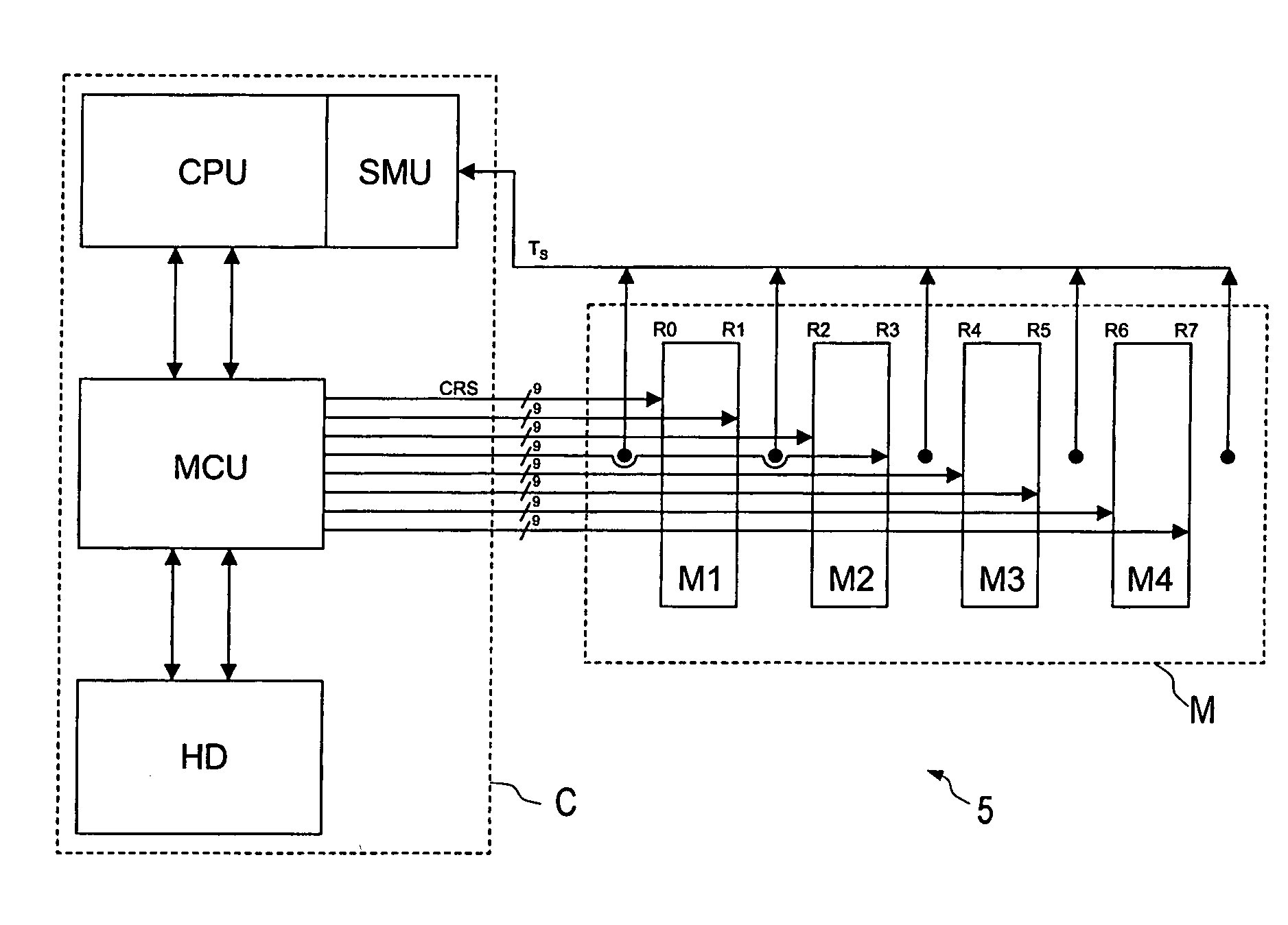
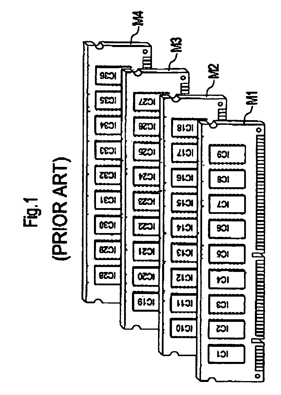
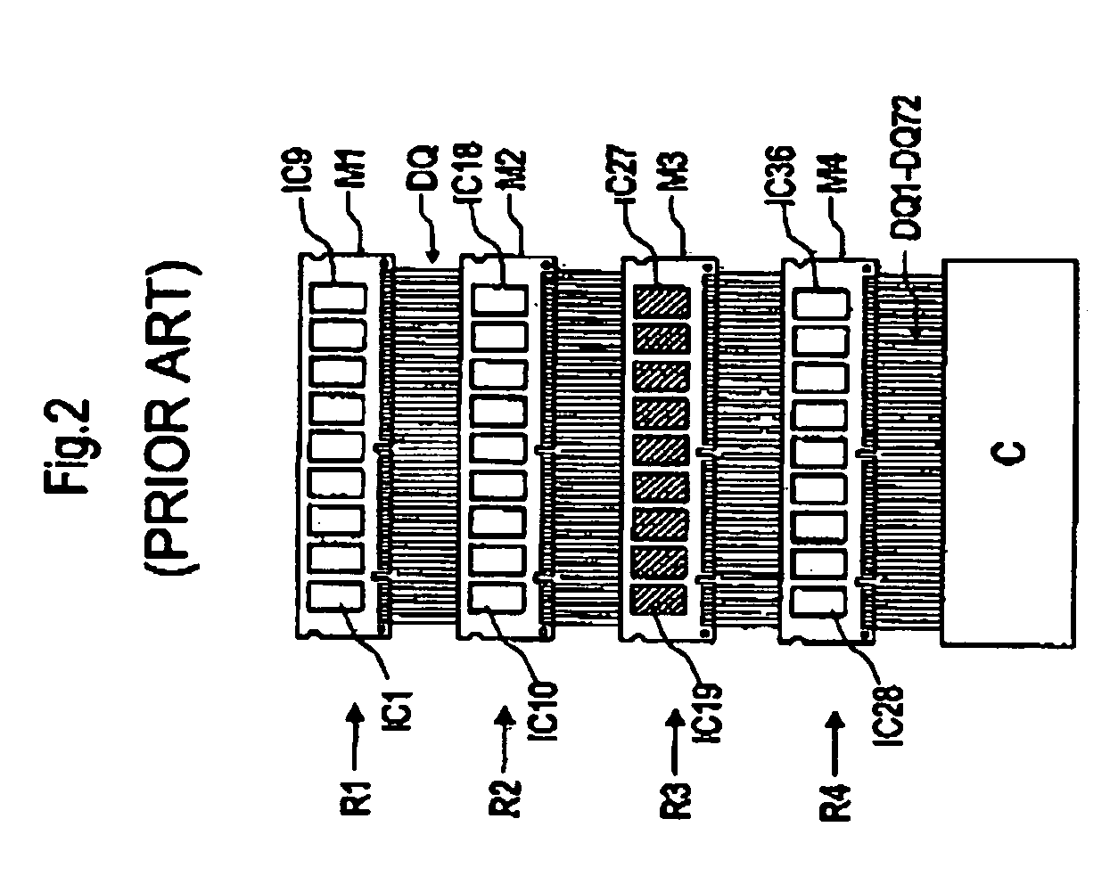
[0036]FIG. 1 shows 36 very similar semiconductor chips IC1–IC36 which are arranged in groups to form nine respective semiconductor chips IC1–IC36 on four very similar modules M1–M4. In this context, the invention makes provision for any semiconductor chips. In the text below, however, the invention is explained by way of example with reference to memory chips which are arranged as DRAM memory chips, such as SDR and DDR SDRAMS, on memory modules, “single in-line memory modules” (SIMM) or “dual in-line memory modules” (DIMM). These memory modules, which are known from the area of computers, in particular, are frequently plugged, in the arrangement shown in FIG. 1, closely together into slots provided for this purpose in a motherboard (not shown in this case) and form the main memory of a computer system. By means of contacts which are preferably arranged along one long edge of a module M1–M4, the modules M1–M4 are connected to the data lines DQ1–DQ72 and also to supply and signal line...


PUM


Abstract

The invention relates to a method for operating semiconductor chips, particularly memory chips, which are arranged in groups on modules which are connected to a common data bus wherein each semiconductor chip on each module is connected to at least one data line in the common data bus comprising the following method steps:a) selecting a group of semiconductor chips from the semiconductor chips arranged on the modules based on a prescribed selection criterion independently of module, the selected group of semiconductor chips using data lines in the common data bus over the entire bus width;b) activating the semiconductor chips in the selected group; andc) performing data interchange between the data lines in the common data bus and the selected group of semiconductor chips.

Description

CROSS-REFERENCE TO RELATED APPLICATIONS[0001]This application claims foreign priority benefits under 35 U.S.C. § 119 to co-pending German patent application number 103 43 525.5 filed Sep. 19, 2003, which claims priority of German patent application number 102 45 272.5 filed Sep. 27, 2002. These related patent applications are herein incorporated by reference in its entirety.BACKGROUND OF THE INVENTION[0002]1. Field of the Invention[0003]The invention relates to a method for controlling semiconductor chips, particularly memory chips, which are arranged in groups on modules. The invention also relates to a control apparatus for carrying out the method.[0004]2. Description of the Related Art[0005]Modern electronic systems normally comprise a multiplicity of semiconductor chips which are used as supports for integrated circuits. The large scale of integration achieved for these circuits using present methods allows a multiplicity of functions to be produced on a single semiconductor chi...

Claims


Application Information

Patent Timeline
IPC IPC(8): G06F17/50G06F9/45G06F13/16G06F15/177G11C7/04G11C11/407
CPCG06F13/1684
Inventor DICKMAN, RORY
Owner POLARIS INNOVATIONS
Why Eureka
Try Eureka