Multiple numerical aperture electron beam projection lithography system

a lithography system and electron beam technology, applied in the field of high-resolution electron beam systems, can solve the problems of large-scale integrated circuits, large variation in beam current and potential degradation of resolution for a single beam, and too low throughput of probe-forming exposure tools, even of the shaped beam type, to achieve the effect of high economic feasibility, high beam current and resolution degradation

Inactive Publication Date: 2002-07-02
NIKON CORP
View PDF5 Cites 15 Cited by
  • Summary
  • Abstract
  • Description
  • Claims
  • Application Information

AI Technical Summary

Problems solved by technology

Therefore, the throughput of probe-forming exposure tools, even of the shaped-beam type, is too low to be economically feasible for high density, large scale integrated circuits even though exposures can be made at relatively high speed.
However, this process and the resulting resist pattern is limited by the ultimate resolution of the electron beam system.
This variation, although more limited than the theoretically possible variation of beam current still represents a wide variation in beam current and potential degradation of resolution for a single numerical aperture, regardless of how it may be optimized.
The effects of the stochastic interactions are not correctable.
However, the beam currents are typically too low (in the pA-nA range) for the effect of stochastic Coulomb interactions to affect resolution of the beam.

Method used


Image

  • Multiple numerical aperture electron beam projection lithography system
  • Multiple numerical aperture electron beam projection lithography system
  • Multiple numerical aperture electron beam projection lithography system

Examples


Embodiment Construction

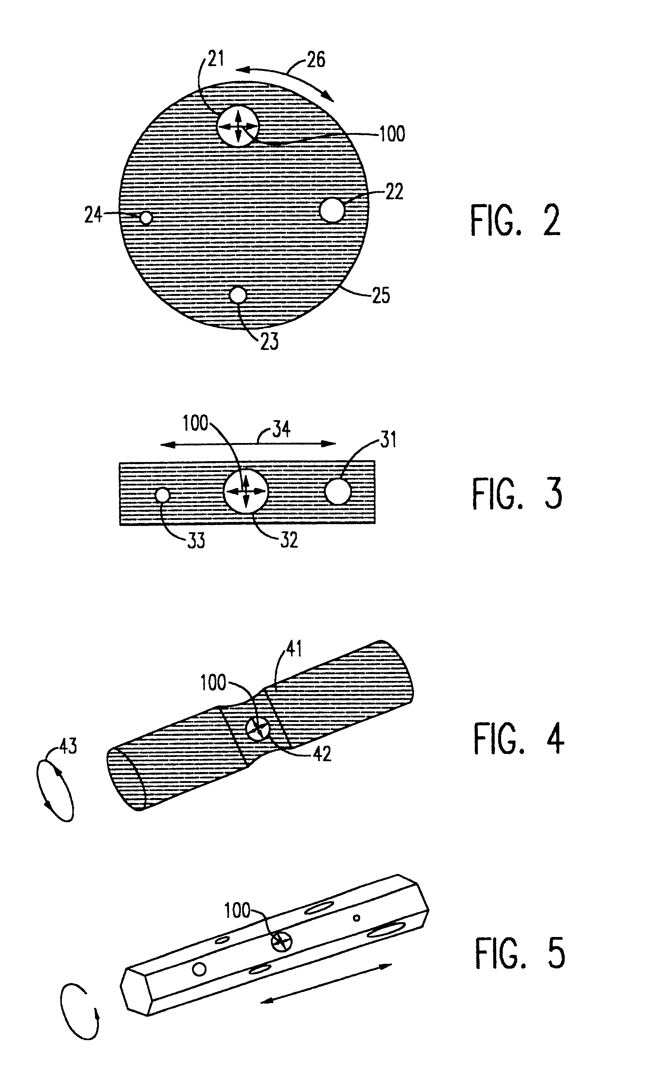
Referring now to the drawings, and more particularly to FIG. 1, there is shown a generalized graphical depiction of the dependence of dimensional resolution on numerical aperture in a charged particle lithography tool for different beam currents. Since the depiction is generalized, no numerical values are indicated on the orthogonal axes. It should also be understood that the term "resolution" refers to the dimensions of a feature which the system can resolve. Thus, the positive direction along the vertical axis of the graph of FIG. 1 represents an increased dimension that can be resolved; corresponding to a resolution value which would be described in some instances as being "lower" or "reduced" resolution. In other words, the optimum resolution for each beam current is represented as a minimum in a respective curve 12, 14 corresponding to a given column configuration. The spherical and chromatic aberration coefficients are fixed for a given charged particle beam column configurati...


PUM

PropertyMeasurementUnit
sizeaaaaaaaaaa
transparencyaaaaaaaaaa
particle trajectory semi-angleaaaaaaaaaa

Abstract

A beam-limiting aperture truncates selected portions of a charged particle beam illuminating portions such as subfields of a patterned reticle of a charged particle beam projection lithography tool and then projects a pattern of charged particles onto a target in a charged particle beam lithography tool. The respective portions of the reticle are patterned in accordance with respective portions of an integrated circuit or other desired pattern and may have differing transmissivities; altering beam current at the target even when source beam current remains substantially constant. The portion of the beam which is truncated, thus altering the particle trajectory semi-angle and numerical aperture of the tool is controlled in accordance with the transmissivity of the reticle portion to enhance resolution to near optimal limits.

Description

1. Field of the InventionThe present invention generally relates to high-resolution electron beam systems and, more particularly, to electron beam projection lithography tools having variable beam current.2. Description of the Prior ArtMany areas of technical endeavor have, in recent years, required increasing levels of dimensional accuracy and resolution. In particular, the field of integrated circuit manufactures has manifested increasing need for increased density of integration and reduced device (e.g. transistors, capacitors, interconnects and the like) dimensions. Reduced device dimensions and increased device proximity provides advantages in both economy of manufacture and level of performance and functionality of integrated circuit chips.These advantages can readily be appreciated when it is considered that the reduction of size and spacing between devices on a chip allows more devices to be formed on a chip or wafer of given size by the same sequence of process steps having...

Claims


Application Information

Patent Timeline
Patent Type & Authority Patents(United States)
IPC IPC(8): H01J37/09H01J37/317G03F7/20H01J37/305H01L21/027
CPCB82Y10/00B82Y40/00H01J37/09H01J37/3174
Inventor GORDON, MICHAEL S.KENDALL, RODNEY A.PINCKNEY, DAVID J.
Owner NIKON CORP
Why Eureka
Try Eureka