Method for manufacturing precision electroplated solder bumps
- Summary
- Abstract
- Description
- Claims
- Application Information
AI Technical Summary
Benefits of technology
Problems solved by technology
Method used
Image
Examples
Embodiment Construction
1. The Preferred Embodiments
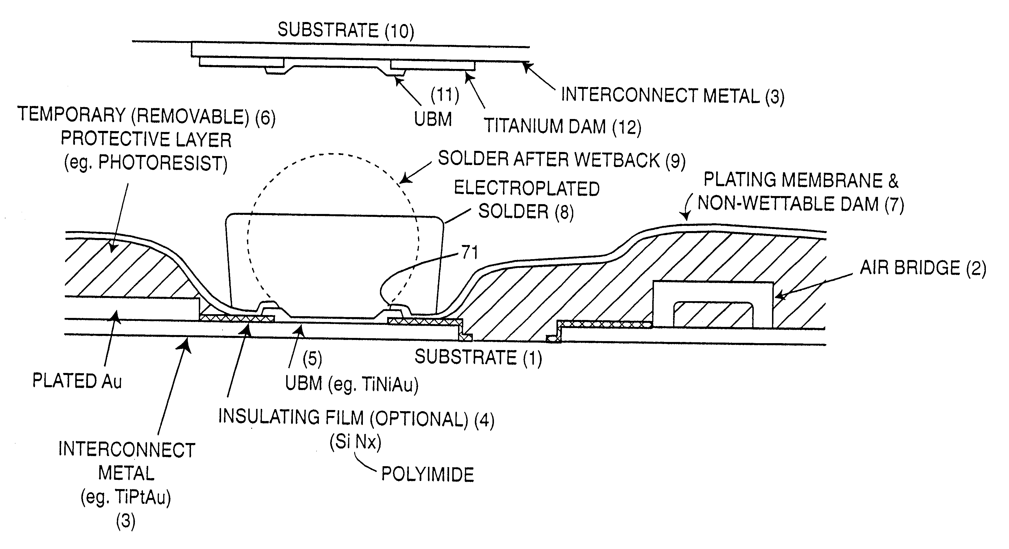
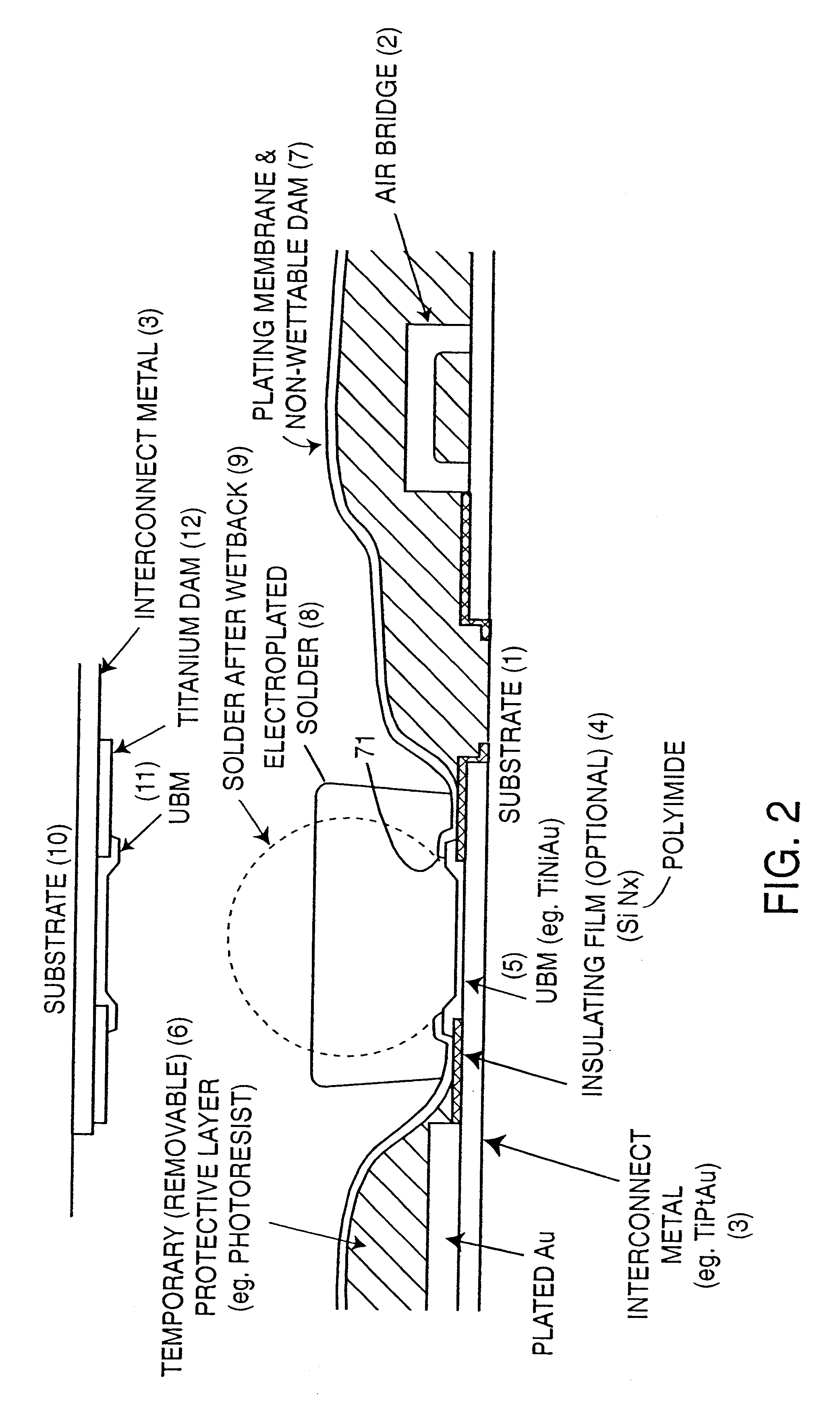
The preferred solder bump structure of this invention is illustrated in FIGS. 2, 2(a), and 3. The structure is formed on a substrate 1 that contains either group IV or group III-V semiconductor devices and circuits. The devices and circuits may contain exposed air bridges 2, microelectromechanical elements such as MEMS switches (not shown), and / or optoelectronic devices with exposed optical surfaces and coatings (not shown, either). These devices and circuits typically utilize exposed gold and / or titanium and / or platinum interconnect lines 3. The solder bump defining structure is a multilayer structure. The first layer is preferably an optional patterned insulating film 4 or a sealant feature on top of which the underbump metallization UBM 5 is applied followed by a patterned layer of a photoresist 6 and, finally, by a thin layer 7 of a metal, preferably, titanium.
Preferably the interconnect 3 is at least partially covered by an insulating film 4 in the v...
PUM
| Property | Measurement | Unit |
|---|---|---|
| thickness | aaaaa | aaaaa |
| thickness | aaaaa | aaaaa |
| thickness | aaaaa | aaaaa |
Abstract
Description
Claims
Application Information
 - R&D
- Intellectual Property
- Life Sciences
- Materials
- Tech Scout
- Unparalleled Data Quality
- Higher Quality Content
- 60% Fewer Hallucinations
Browse by: Latest US Patents, China's latest patents, Technical Efficacy Thesaurus, Application Domain, Technology Topic, Popular Technical Reports.
© 2025 PatSnap. All rights reserved.Legal|Privacy policy|Modern Slavery Act Transparency Statement|Sitemap|About US| Contact US: help@patsnap.com


