Confinement of E-fields in high density ferroelectric memory device structures

a high-density ferroelectric memory and field technology, applied in the direction of semiconductor devices, capacitors, electrical devices, etc., can solve the problems of deleterous effects, and achieve the effect of preventing short-circuiting

Inactive Publication Date: 2002-01-29
FELLOWS RES B V
View PDF7 Cites 8 Cited by
  • Summary
  • Abstract
  • Description
  • Claims
  • Application Information

AI Technical Summary

Benefits of technology

The present invention relates generally to structures and methods for confining E-fields in high-density ferroelectric memory applications to minimize unwanted dispersion of the E-field into regions surrounding the ferroelectric material.
(b) patterning the stack capacitor, depositing an insulating capping layer on the patterned stack capacitor to prevent electrical short-circuiting between top and bottom electrodes of the stack capacitor, and depositing a conducting layer over and on the sides of the stack capacitor;

Problems solved by technology

This effect of losses in switched charge will tend to increase the voltage needed to switch the ferroelectric, and it will also project the applied E-fields into adjacent memory cells, with the potential result of undesired interference.
Such effect may also distribute the E-fields non-uniformly within the ferroelectric layer, with deleterious effects.

Method used


Image

  • Confinement of E-fields in high density ferroelectric memory device structures
  • Confinement of E-fields in high density ferroelectric memory device structures

Examples


Embodiment Construction

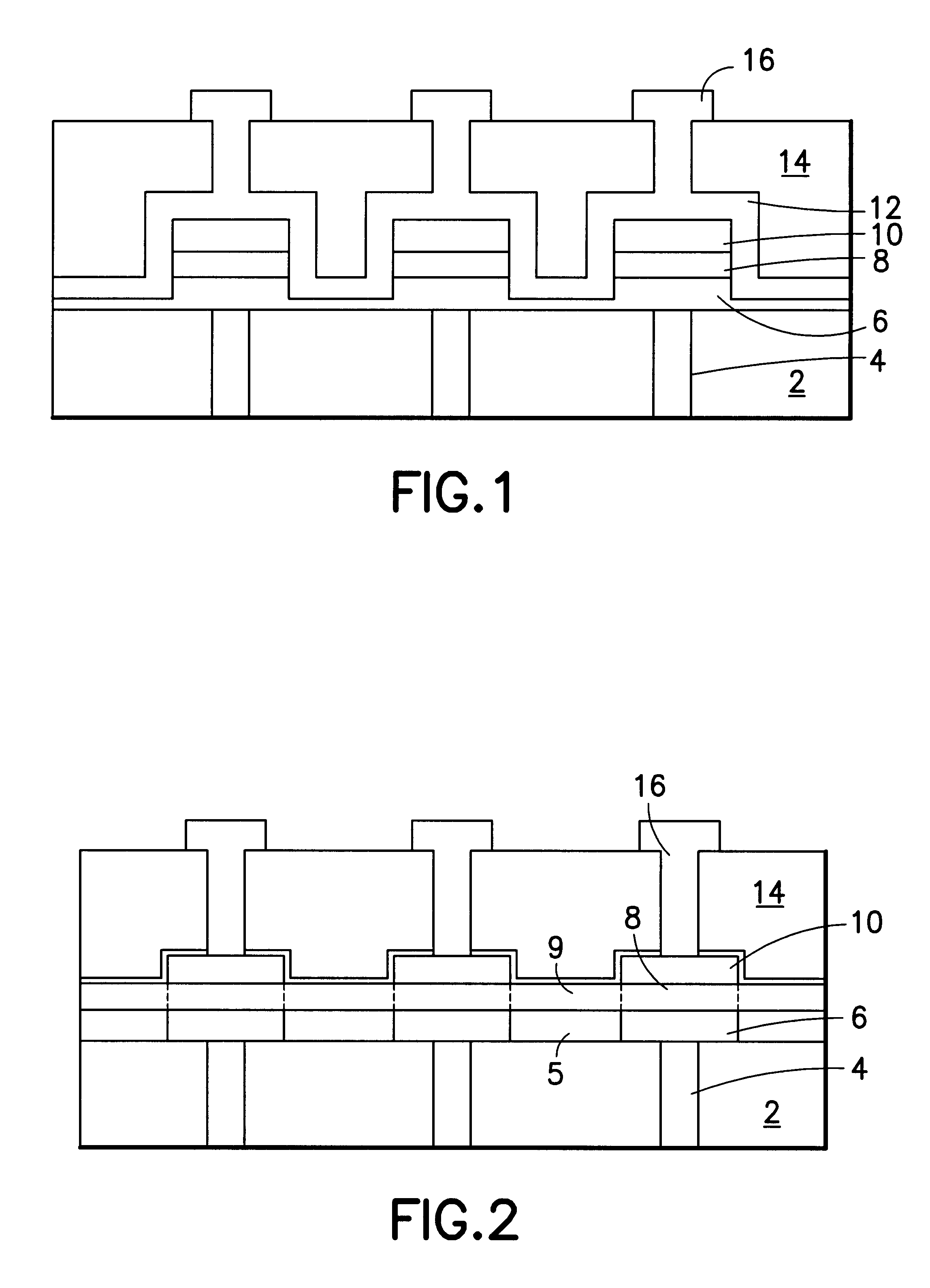
The present invention contemplates various approaches to prevent unwanted dispersion of the E-fields into the regions that surround the ferroelectric material that needs to be switched in the operation of the ferroelectric device. These approaches are described in greater detail below.

One such approach includes the deposition of a non-ferroelectric, high permittivity insulating layer over and on the sides of the previously patterned capacitor stack in a capacitor precursor structure comprising such stack.

The non-ferroelectric, high permittivity insulating layer in such approach may be formed of any suitable material, as for example, TiO.sub.2 (.di-elect cons..apprxeq.90), Ta.sub.2 O.sub.5 (.di-elect cons..apprxeq.40), barium strontium titanate (BST) or doped BST (.di-elect cons..apprxeq.400). Alternatively, the non-ferroelectric, high permittivity insulating layer may be formed of a non-ferroelectric doped or modified lead zirconium titanate (PZT) material such as Pb.sub.0.09 La.sub...


PUM


Abstract

A ferroelectric capacitor device structure, including a ferroelectric stack capacitor comprising a ferroelectric material capacitor element on a substrate containing buried transistor circuitry beneath an insulator layer having a via therein containing a conductive plug to the transistor circuitry, wherein E-fields are structurally confined to the ferroelectric capacitor material element. Such E-fields confinement may be effected by fabrication of the device structure including: (a) patterning the stack capacitor, and depositing a non-ferroelectric, high ∈ material layer over and on the sides of the stack capacitor; (b) forming the stack capacitor without patterning the ferroelectric material and rendering a portion of the material non-ferroelectric in character; or (c) forming the ferroelectric stack capacitor with an aspect ratio, of effective lateral dimension d of the ferroelectric capacitor material element to thickness t of the ferroelectric capacitor material element, that is greater than 5, with d and t being measured in same dimensional units.

Description

1. Field of the InventionThis invention relates generally to structures and methods for confining E-fields in high-density ferroelectric memory applications, so that unwanted dispersion of the E-field into regions surrounding the ferroelectric material is avoided.2. Description of the Related ArtThere is a major effort by semiconductor companies throughout the world to commercialize ferroelectric thin films in advanced dynamic random access memories (DRAMs) and ferroelectric random access memories (FeRAMs), respectively.Ferroelectric thin film materials of interest for such FeRAM applications include PbZrTiO.sub.3 (PZT) and SrBi.sub.2 Ta.sub.2 O.sub.9 (SBT). While the majority of current efforts are directed to the commercial development of relatively large capacitors (e.g. 5 .mu.m.sup.2 area), the ultimate goal is to adapt ferroelectric random access memory technology for future generations of integrated circuit devices in which capacitor areas, cell sizes and voltages are scaled d...

Claims


Application Information

Patent Timeline
Patent Type & Authority Patents(United States)
IPC IPC(8): H01L21/02H01L21/285
CPCH01L28/75H01L21/28518H01L28/55H01L21/28568
Inventor VAN BUSKIRK, PETER C.BILODEAU, STEVEN M.
Owner FELLOWS RES B V
Why Eureka
Try Eureka