Semiconductor wafer etching method
- Summary
- Abstract
- Description
- Claims
- Application Information
AI Technical Summary
Benefits of technology
Problems solved by technology
Method used
Image

Examples
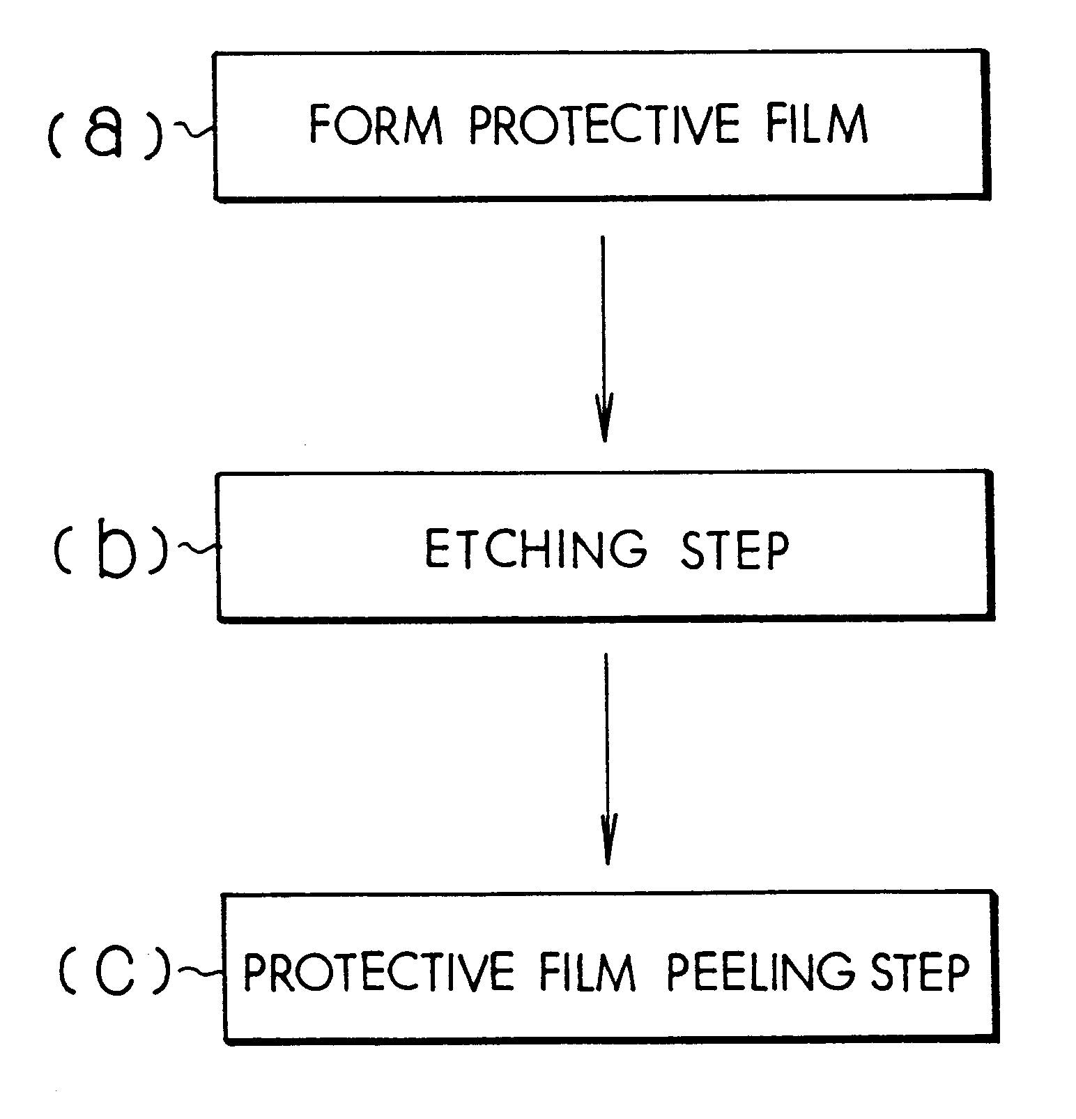
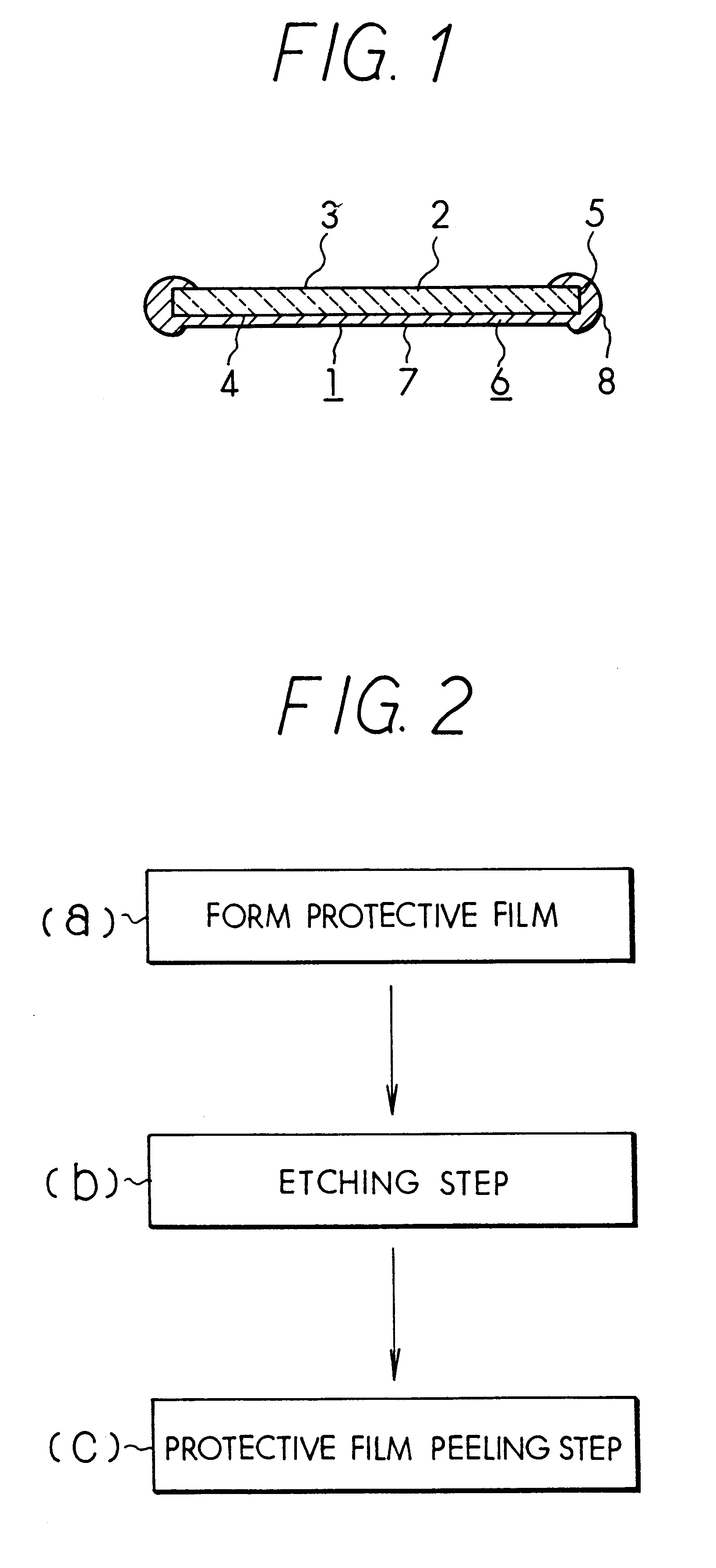
first embodiment
the present invention will be described with reference to FIG. 1.
FIG. 1 shows a semiconductor wafer body 1 comprising a semiconductor wafer 2 and a protective film 6. The protective film 6 is placed on the opposite side of the wafer 2 relative to the wafer surface (hereinafter etching surface) 3, which in the etching method is etched for forming a thin section (not shown in the Figure) for the Si diaphragm, etc. The non-etched circumference of the semiconductor wafer body 1 is represented by numeral 5, while numeral 7 represents the rear protective film formed over pattern surface 4, while numeral 8 is the circumference of a protective film covering side circumference 5 and rim excluding the etching section, thereby forming protective film 6.
In this embodiment, semiconductor wafer 2 from which protective film 6 is peeled and cleaned after passing through the alkali etching process in the above state is obtained (not shown in the Figure).
This type of etching method is explained below...
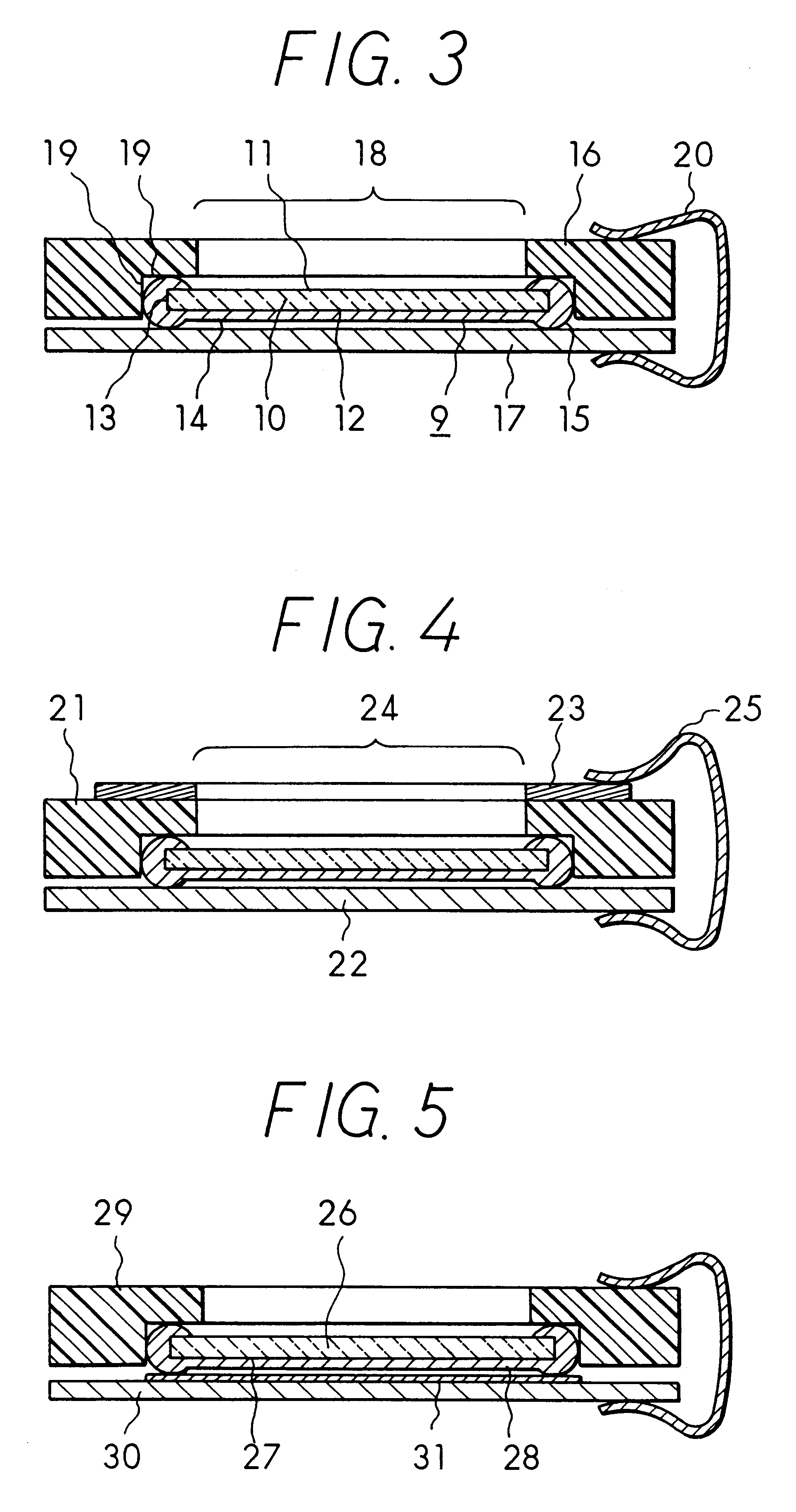
second embodiment
the present invention will now be described. In the semiconductor wafer with protective film etched as in the first embodiment, the sealing of the silicon resin protective film and semiconductor wafer was sufficient as seen with the amount of etching fluid that infiltrated the film in the test. However, if an alkali resistant resin such as terpene or polystyrene, etc., or de-alcohol silicon resin was used, the sealing properties dropped somewhat, thus creating the risk that a large amount of etching fluid may enter. Thus it is necessary to securely avoid the risk that the etching fluid may enter when using those materials having an inferior sealing property.
The present inventors performed assorted inspections and evaluations on the etching fluid infiltration from the clearances between the protective film and semiconductor wafer. As a result, a method to increase the sealing force between the protective film and semiconductor wafer to prevent infiltration of etching fluid was realiz...
PUM
| Property | Measurement | Unit |
|---|---|---|
| Thickness | aaaaa | aaaaa |
| Force | aaaaa | aaaaa |
| Pressure | aaaaa | aaaaa |
Abstract
Description
Claims
Application Information
 - R&D
- Intellectual Property
- Life Sciences
- Materials
- Tech Scout
- Unparalleled Data Quality
- Higher Quality Content
- 60% Fewer Hallucinations
Browse by: Latest US Patents, China's latest patents, Technical Efficacy Thesaurus, Application Domain, Technology Topic, Popular Technical Reports.
© 2025 PatSnap. All rights reserved.Legal|Privacy policy|Modern Slavery Act Transparency Statement|Sitemap|About US| Contact US: help@patsnap.com