
Conduction assist member and manufacturing method of the same

Inactive Publication Date: 2001-03-20
NGK INSULATORS LTD
View PDF17 Cites 97 Cited by
  • Summary
  • Abstract
  • Description
  • Claims
  • Application Information

AI Technical Summary

Problems solved by technology

However, if the connecting element has a distortion, or dust or the like exists between the connecting elements, the contact area between the connecting elements becomes small.
As a result, close contact between the connecting elements is prevented and electrical connection becomes incomplete.
However, the above-mentioned conduction assist member is used in a socket-plug type connector and especially the conduction assist member as disclosed in Japanese Utility Model Publication (Kokoku) No. 51-8710 has a problem in durability such that the tongue pieces or blade portions are damaged or abraded due to repeated use.
Furthermore, the conduction assist member has a problem that it must be prepared in compliance with different standards so that it matches with sizes of connectors.
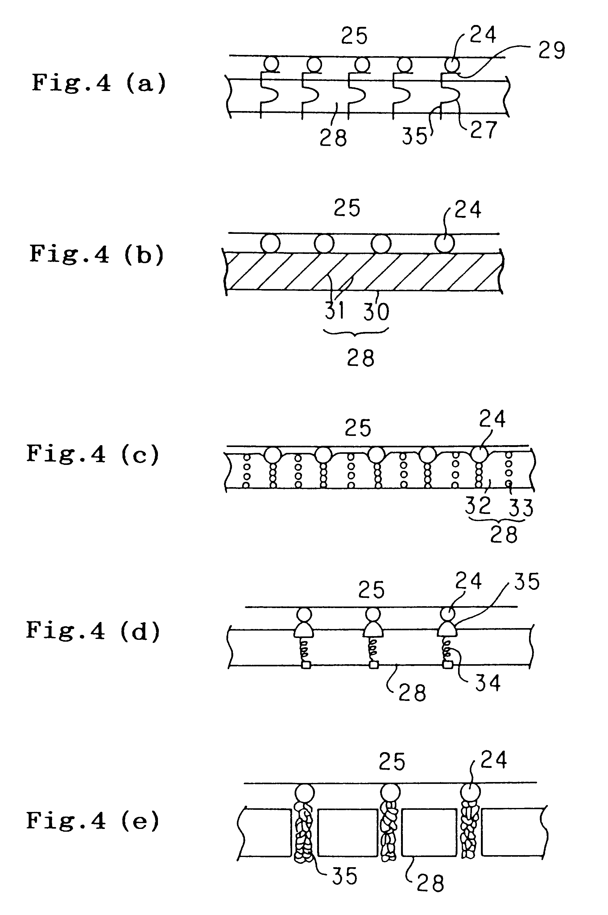
As to the contact substrates for integrated circuits, the contact substrate shown in FIG. 4(a) is inferior in high speed performance and poses a problem that it cannot be used for an integrated circuit socket for mounting.
Also, with respect to the contact substrate shown in FIG. 4(c), there are problems that conduction is unstable due to a fact that the conductive grains 33 in a line are not brought into sufficient contact with each other or are brought into contact with the conductive grains 33 in another line.
Further, since the contact substrate shown in FIG. 4(d) is required to be thick inevitably due to the structure thereof, it exhibits problems in that it exhibits inferior high speed performance and that it is not suited for mounting use.
Furthermore, the contact substrate shown in FIG. 4(e) poses a problem that it has diversified conduction paths and its electric characteristics become unstable.

Method used


Image

  • Conduction assist member and manufacturing method of the same
  • Conduction assist member and manufacturing method of the same
  • Conduction assist member and manufacturing method of the same

Examples


example

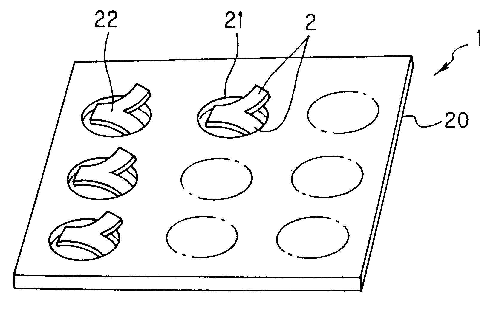
A conduction assist member in which cut pieces are bent in two directions as shown in FIG. 7 was manufactured by a method described below.

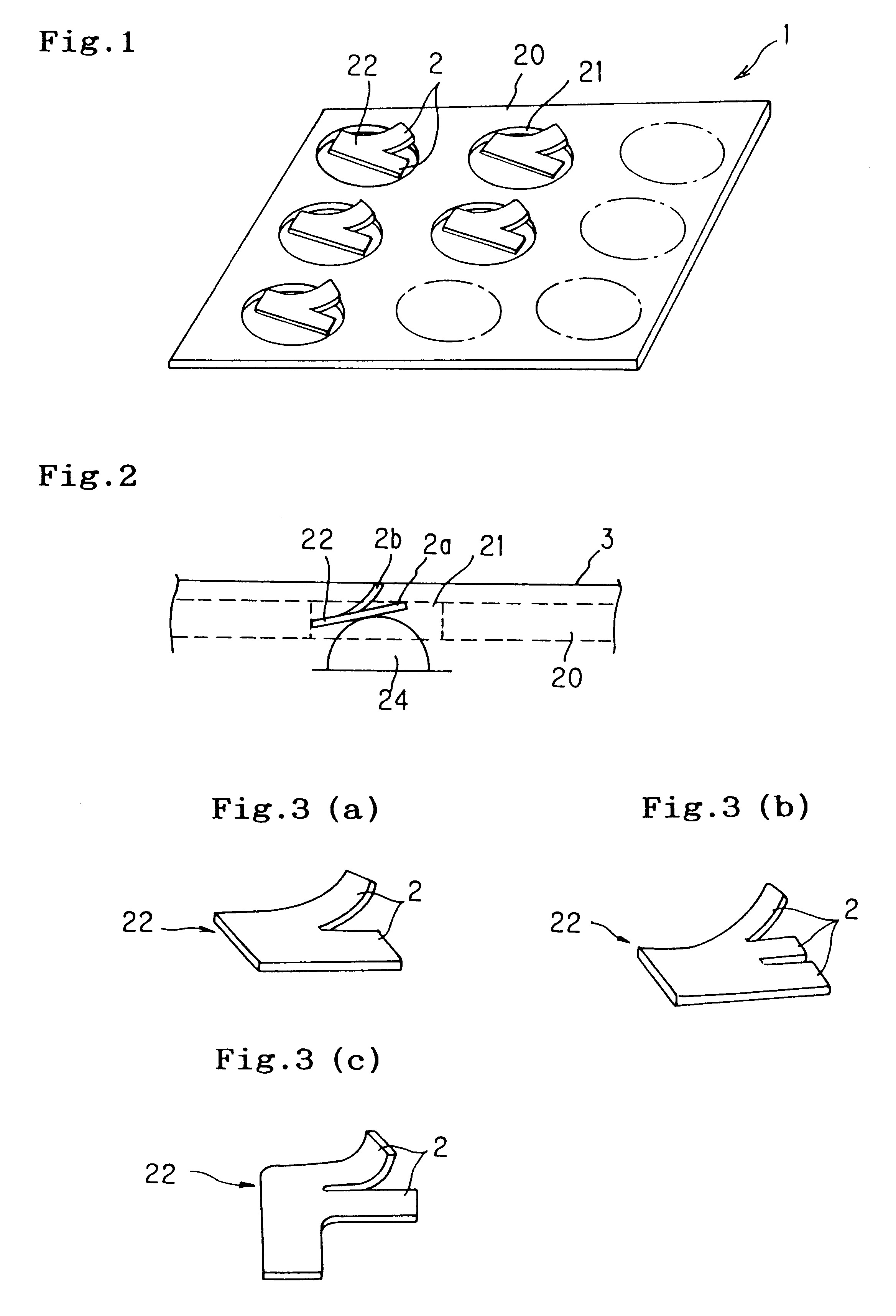
By etching a sheet having a layer 5 made of beryllium copper, cut pieces 22 each having a cut were formed at a pitch of 0.5 mm on one surface of a polyimide film 39a with a length of 50 mm, a width of 50 mm and a thickness of 0.125 mm as shown in FIG. 6(a).

Next, the cut pieces 22 were covered by laminating another film 39b which is made of polyimide and has the same size with the film 39a as shown in FIG. 6(b) and a sheet 20 was formed by bringing the two films into thermal press contact.

Next, as shown in FIG. 6(c), through holes 21 which had a diameter of 0.5 mm were formed at a pitch of 0.5 mm by removing the film in the vicinities of the cut pieces 22 with a laser.

Finally, punching was made to each through hole 21 in two directions so that two blades 2 formed on each cut piece 22 were bent in directions opposite to each other as shown in FIG. 8...


PUM


Abstract

A conduction assist member has conductive members disposed in some or all through holes which are formed in a large number in a sheet made of an insulating elastic material. The conduction member is a cut piece which is fixed to the sheet at one end thereof and has two or more blades formed by one, two or more cuts. In the conduction assist member, one or some of the two or more blades formed on each cut piece, are bent toward one of two opening portions of the through hole so that ends of the blades formed on the cut pieces protrude from the opening portion on the same surface of the sheet. The conduction assist member can be applied as a connector to both a flat conduction surface and a curved conduction surface, and as an integrated circuit socket which can easily cope with differences in sizes of connectors and sockets, which is superior in high speed performance and usable as an integrated circuit socket for mounting, and which can easily be assembled.

Description

BACKGROUND OF THE INVENTION AND RELATED ART STATEMENTThe present invention relates to a conduction assist member used for connection between conductors for various electronic equipments, manufacturing method of the same, a connector using the same and an integrated circuit socket using the same.A conduction assist member functions to assist electrical conduction between connecting elements of a connector by being made to intervene between the connecting elements.There are several types of connector electrically connecting conductors to each other. For example, in one type of connector, connecting elements have flat conductive surfaces. They are laid one on top of the other and brought into contact with each other so that electrical conduction is made. In another type of connector, one of connecting elements is a plug and the other is a socket, and the plug is fitted in the socket to bring an outer circumferential surface of the plug into contact with an inner circumferential of a so...

Claims


Application Information

Patent Timeline
IPC IPC(8): H01R13/03H01R43/16H01R43/20H01R12/00
CPCH01R13/03H01R43/16H01R43/20H01R9/091
Inventor OCHIAI, TOSHIMASA
Owner NGK INSULATORS LTD
Learn More