Method of detecting end point of polishing of wafer and apparatus for detecting end point of polishing
a technology of end point and end point, which is applied in the direction of manufacturing tools, semiconductor/solid-state device testing/measurement, and lapping machines, etc., can solve the problems of data scattered, poor accuracy can be obtained, and poor accuracy of flattening
- Summary
- Abstract
- Description
- Claims
- Application Information
AI Technical Summary
Problems solved by technology
Method used
Image

Examples
Embodiment Construction
The present invention will now be described in detail with reference to the accompanying drawings. (Wafer to be processed)
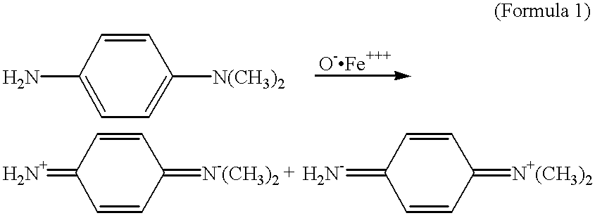
A wafer to be processed of the present invention has a substrate made of silicon, an alumina-titanium carbide alloy or LCD glass. A permalloy magnetic layer made of, for example, Ni--Fe, Mn--Fe, Co--Fe, Ni--Rh--Fe, Co--Zr--Fe or Co--Fe--B is formed on the surface of the foregoing substrate. If necessary, a circuit made of Cu, Ag or Au is formed thereon. Then, an insulating layer made of aluminum oxide or the like is formed so that the wafer is formed. Also the present invention may be applied to a substrate for a device incorporating an interlayer insulating film made of aluminum oxide, silicon dioxide or titanium oxide on which a metal film made of titanium or titanium-aluminum is formed.
(CMP Polishing apparatus)
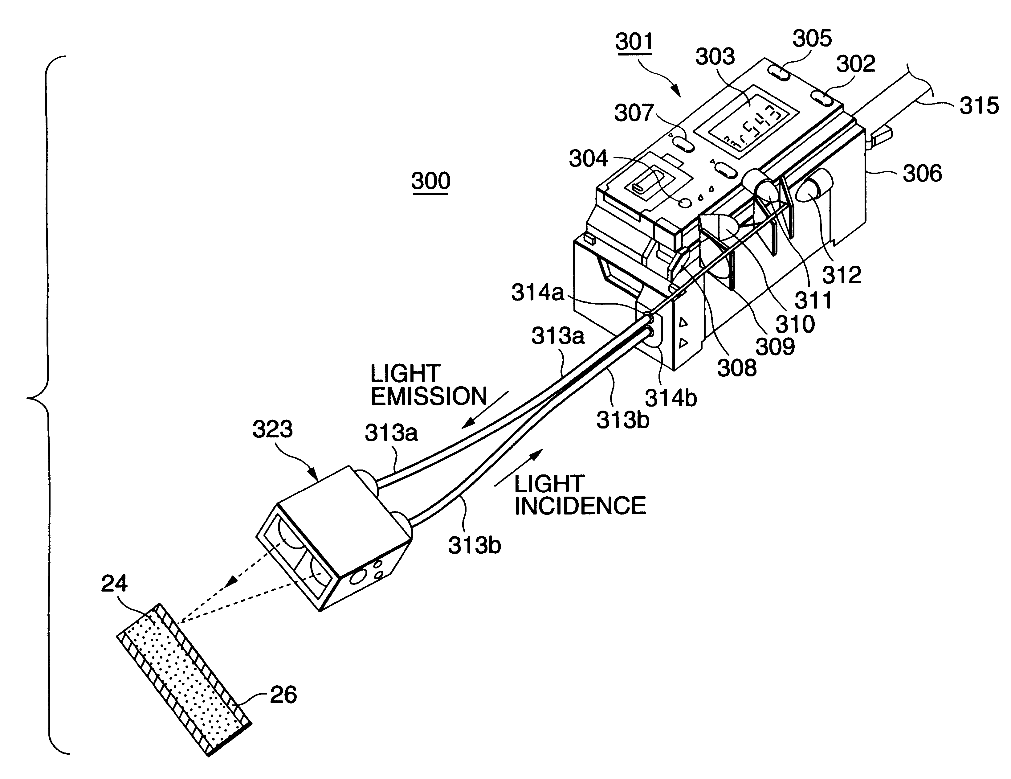
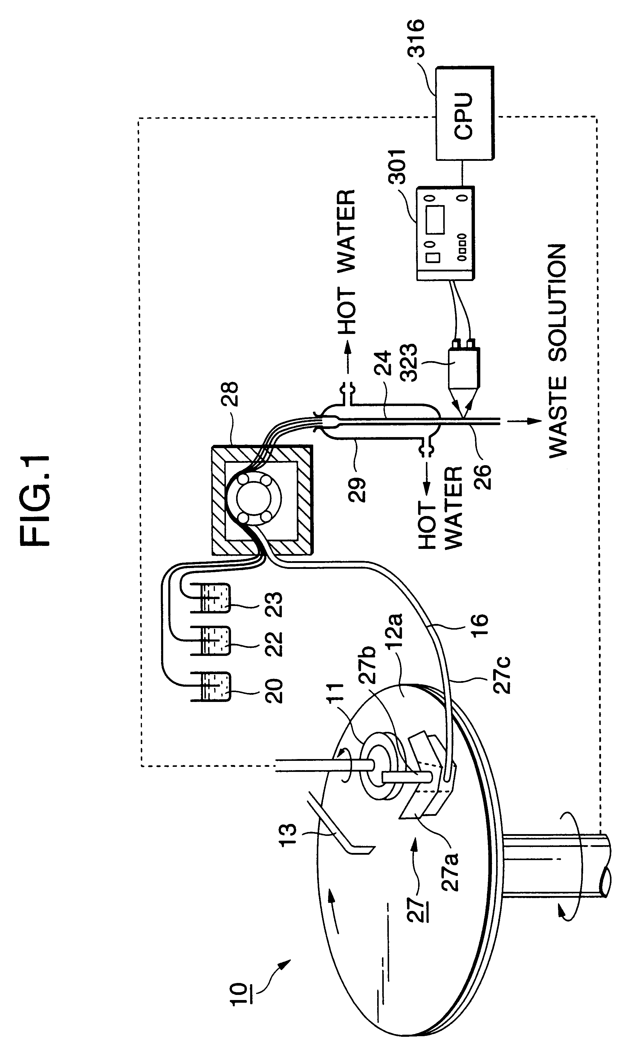
FIG. 3 shows a CMP polishing apparatus 10 of the present invention. In the CMP polishing apparatus 10, a wafer "w" is vacuum-adsorbed to a chuck table (...
PUM
| Property | Measurement | Unit |
|---|---|---|
| Flow rate | aaaaa | aaaaa |
| Color | aaaaa | aaaaa |
| aaaaa | aaaaa |
Abstract
Description
Claims
Application Information
 - R&D
- Intellectual Property
- Life Sciences
- Materials
- Tech Scout
- Unparalleled Data Quality
- Higher Quality Content
- 60% Fewer Hallucinations
Browse by: Latest US Patents, China's latest patents, Technical Efficacy Thesaurus, Application Domain, Technology Topic, Popular Technical Reports.
© 2025 PatSnap. All rights reserved.Legal|Privacy policy|Modern Slavery Act Transparency Statement|Sitemap|About US| Contact US: help@patsnap.com