
Carrier based high volume system level testing of devices with pop structures

a carrier-based, high-volume technology, applied in the direction of measurement devices, electronic circuit testing, instruments, etc., can solve the problems of increased cost (both an initial set-up cost and maintenance cost) of high-speed signal path calibration, easy implementation of shielding and other top-side contact solutions, and simplified system design. , the effect of improving reliability

Active Publication Date: 2022-09-08
ADVANTEST TEST SOLUTIONS INC
View PDF11 Cites 4 Cited by
  • Summary
  • Abstract
  • Description
  • Claims
  • Application Information

AI Technical Summary

Benefits of technology

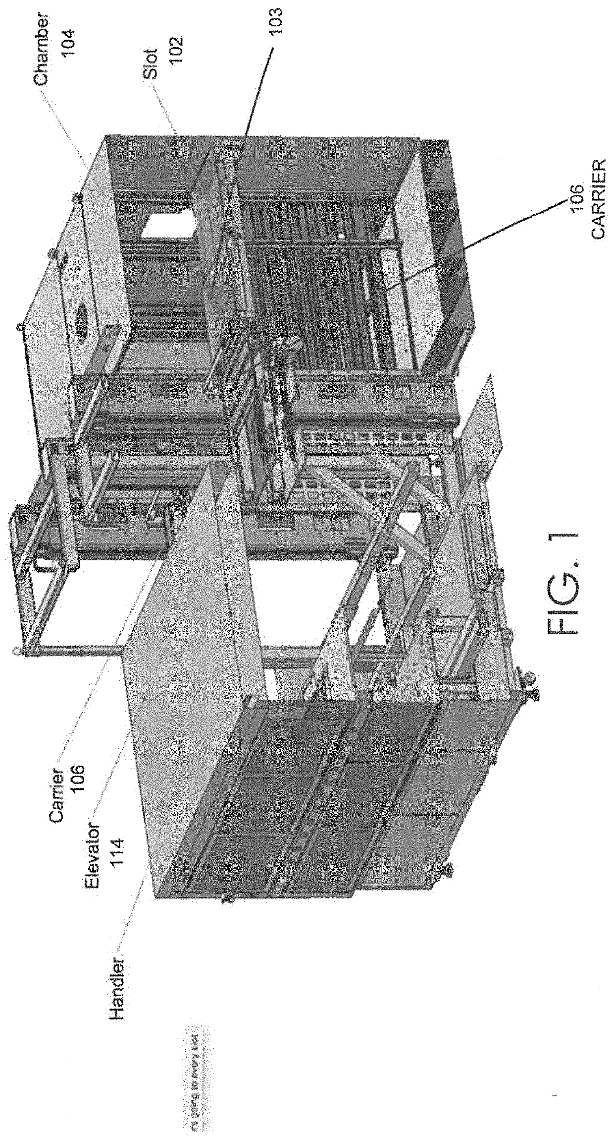
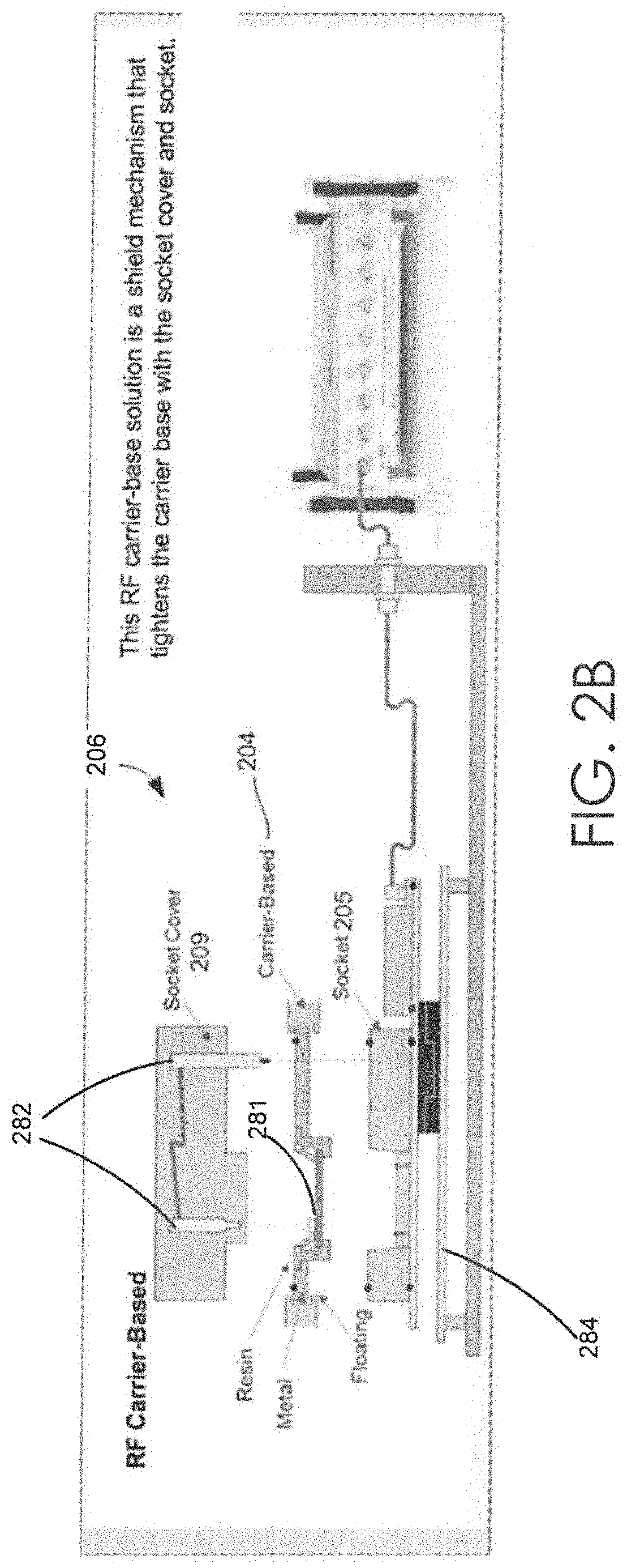
[0009]Accordingly, there is a need for an ATE system that addresses the drawbacks associated with conventional ATE tester systems. Embodiments of the present invention provide a massively parallel high-volume test capability in a slot-based architecture, using multi-device passive carriers to transport the semiconductor devices from the loading / unloading station to the test slots. This eliminates the requirement to move the test sockets and / or test circuitry with the devices, which is the method used in the current state-of-the-art high-volume slot-based test systems. Eliminating this requirement simplifies the design of the system and provides improved performance (especially for RF and other high frequency applications), improved reliability, and reduced cost.
[0013]A POP memory nest comprises a structure that enables temporary electrical contact of a memory chip with a DUT (Device Under Test) in a vertically stacked POP (Package-on-Package) configuration. The structure may also provide a thermal conductivity path from a thermal head through the memory to the DUT. The POP memory nest is typically composed of a memory chip, an interposer layer that provides electrical conductivity between the contacts on the memory chip and the DUT while protecting the memory chip from damage during repeated contacting cycles, and a frame structure that houses the memory chip and interposer layer and has features for precise alignment with the socket containing the DUT during testing. While the structure typically interfaces a memory device with a processor device, it may also be a different nest that has an RF device stacked on top of a digital device.

Problems solved by technology

Typically, the end result of a test is either “pass” if the device successfully provides certain expected responses within pre-established tolerances, or “fail” if the device does not provide the expected responses within the pre-established tolerances.
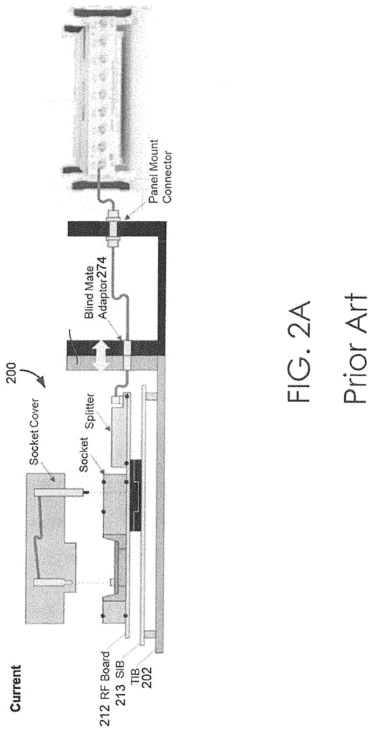
For example, the high-frequency signal path between the socket (per DUT) test circuitry and the equipment in a test rack is repeatedly disconnected during normal test operation, making maintenance of signal fidelity and high-speed signal path calibration difficult.
Further, there is an increased cost (both an initial set-up cost and maintenance costs) for high cycle count high-frequency connectors between a TIB and a test rack.
Further, shielding and other top-side contact solutions are easy to implement due to available space.
Nevertheless, this type of ATE systems also has its drawbacks.
For example, parallelism and Units Per Hour (UPH) (units tested per hour) is severely limited so this type of ATE system is unsuitable for high-volume manufacturing (HV) applications.
Further, there is a low utilization of the expensive pick-and-place apparatus, which often sits idle when the test time is long.
Again, there are drawbacks associated with this type of system.
For example, the per-slot pick and place assemblies increase system cost.
Further, there is a low utilization of per-slot pick-and-place assemblies, which often sit idle when test time is long.
These types of ATE systems may also potentially be unreliable due to multiple pick-and-place assemblies.
The disadvantage with this system is that memory testers and handlers specifically work only with memory and do not incorporate shields for RF or any type of top-side contact.
Further, space requirements for System Level Test (SLT) test circuitry and lack of any vertically-stacked slot architecture limit parallelism.

Method used


Image

  • Carrier based high volume system level testing of devices with pop structures
  • Carrier based high volume system level testing of devices with pop structures
  • Carrier based high volume system level testing of devices with pop structures

Examples


Embodiment Construction

[0029]Reference will now be made in detail to embodiments, examples of which are illustrated in the accompanying drawings. While the embodiments will be described in conjunction with the drawings, it will be understood that they are not intended to limit the embodiments. On the contrary, the embodiments are intended to cover alternatives, modifications and equivalents. Furthermore, in the following detailed description, numerous specific details are set forth in order to provide a thorough understanding. However, it will be recognized by one of ordinary skill in the art that the embodiments may be practiced without these specific details. In other instances, well-known methods, procedures, components, and circuits have not been described in detail as not to unnecessarily obscure aspects of the embodiments.

Notation and Nomenclature Section

[0030]Some regions of the detailed descriptions which follow are presented in terms of procedures, logic blocks, processing and other symbolic repr...


PUM


Abstract

A testing apparatus comprises a tester comprising a plurality of racks, wherein each rack comprises a plurality of slots, wherein each slot comprises: (a) an interface board affixed in a slot of a rack, wherein the interface board comprises test circuitry and a plurality of sockets, each socket operable to receive a device under test (DUT); and (b) a carrier comprising an array of DUTs, wherein the carrier is operable to displace into the slot of the rack; and (c) an array of POP memory devices, wherein each POP memory device is disposed adjacent to a respective DUT in the array of DUTs. Further, the testing apparatus comprises a pick-and-place mechanism for loading the array of DUTs into the carrier and an elevator for transporting the carrier to the slot of the rack.

Description

CROSS-REFERENCE TO RELATED APPLICATIONS[0001]This application also claims priority to U.S. Provisional Application 63 / 158,082 titled “Carrier Based High Volume System Level Testing of Devices with Pop Structures,” filed on Mar. 8, 2021. The entire content of the above-listed application is hereby incorporated by reference for all purposes as if fully set forth herein.FIELD OF THE INVENTION[0002]The present disclosure relates generally to the field of automated test equipment and more specifically to techniques for massively parallel high-volume testing of devices under test.BACKGROUND OF THE INVENTION[0003]Automated test equipment (ATE) includes any testing assembly that performs a test on a semiconductor wafer or die, an integrated circuit (IC), a circuit board, or a packaged device such as a solid-state drive. ATE assemblies may be used to execute automated tests that quickly perform measurements and generate test results that can then be analyzed. An ATE assembly may be anything ...

Claims


Application Information

Patent Timeline
Patent Type & Authority Applications(United States)
IPC IPC(8): G11C29/56G01R31/28G01R31/319
CPCG11C29/56016G01R31/2867G01R31/2863G01R31/31905G11C2029/5602G01R31/2896G01R31/2893
Inventor RANGANATHAN, KARTHIKCRUZAN, GREGORYKABBANI, SAMEROSEGUERA, GILBERTOLEVENTHAL, IRA
Owner ADVANTEST TEST SOLUTIONS INC
Learn More