Ceramic structure, electrostatic chuck and substrate fixing device
- Summary
- Abstract
- Description
- Claims
- Application Information
AI Technical Summary
Benefits of technology
Problems solved by technology
Method used
Image
Examples
first embodiment
[0026][Structure of Substrate Fixing Device]
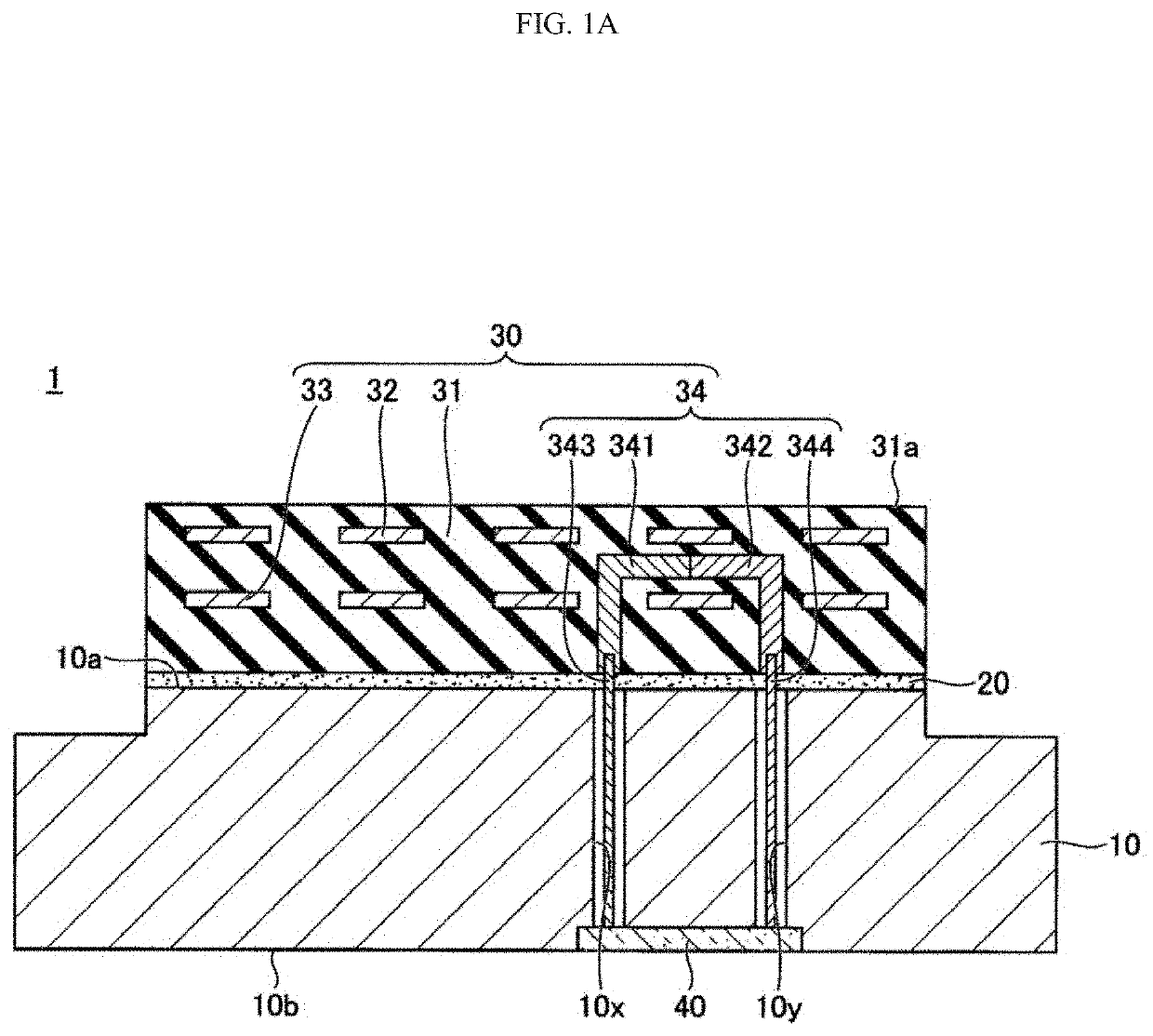
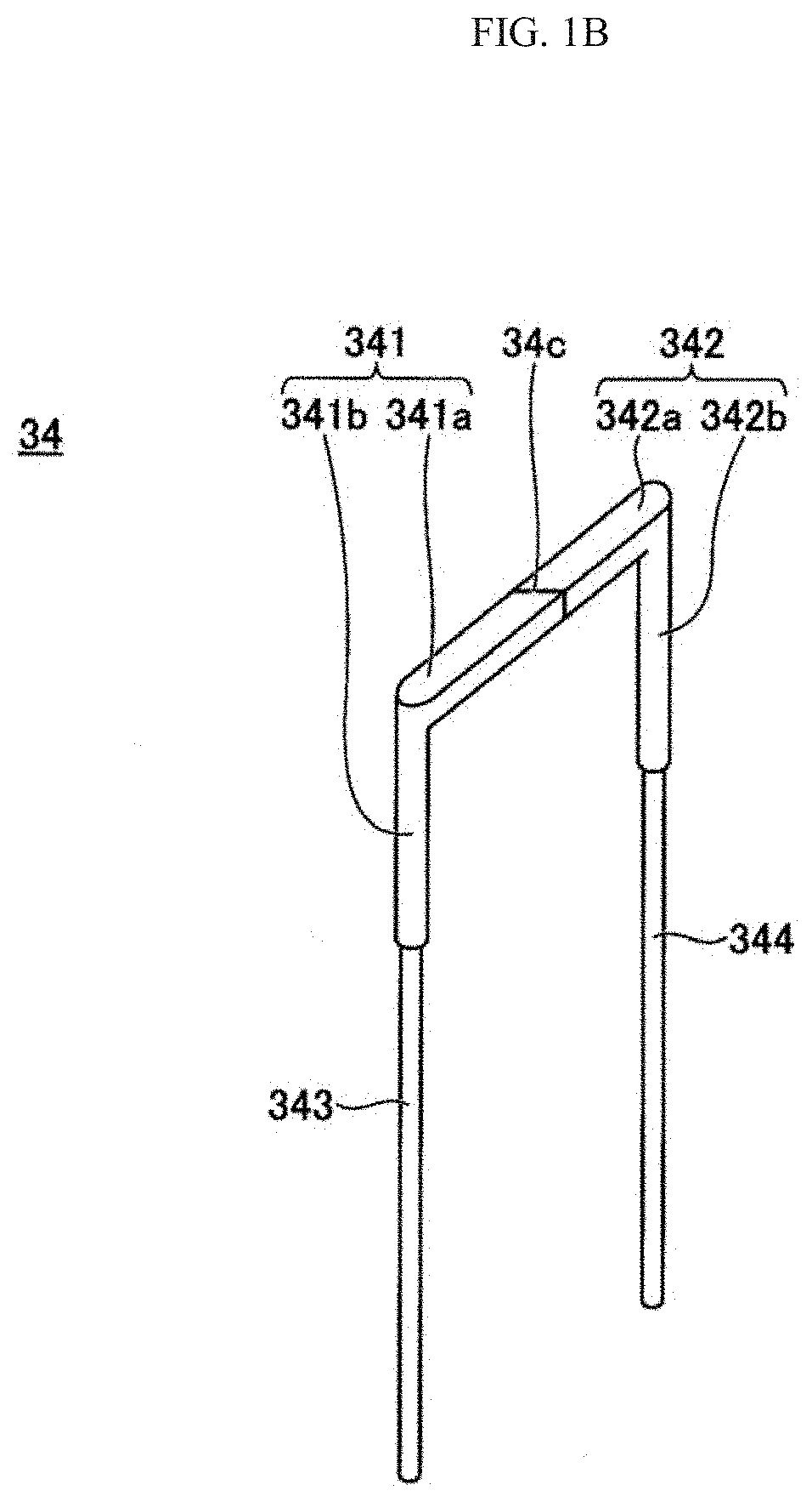
[0027]FIG. 1A is a simplified view showing a substrate fixing device according to a first embodiment, where FIG. 1A is a sectional view and FIG. 1B is a partially enlarged view showing only a thermocouple.
[0028]Referring to FIG. 1A, a substrate fixing device 1 includes, as main constitutional elements, a base plate 10, an adhesion layer 20, an electrostatic chuck 30, and a control unit 40. The substrate fixing device 1 is a device configured to suck and hold a substrate (a wafer and the like), which is a suction target, by the electrostatic chuck 30 mounted on one surface 10a of the base plate 10.
[0029]The base plate 10 is a member for mounting the electrostatic chuck 30. A thickness of the base plate 10 is, for example, about 20 mm to 40 mm. The base plate 10 is formed of, for example, a metal material such as aluminum and cemented carbide alloy, a composite material of the metal material and a ceramic material, or the like, and can be us...
second embodiment
[0089]In a second embodiment, an example of a thermoelectric component having a ceramic substrate and a thermoelectric device is described. Note that, in the second embodiment, the descriptions of the same constitutional components as those in the above-described embodiment may be omitted.
[0090]FIG. 4A is a view showing a thermoelectric component according to a second embodiment, where FIG. 4A is a perspective view and FIG. 4B is a sectional view. As shown in FIG. 4A, a thermoelectric component 5 is a ceramic structure having a ceramic substrate 51 that is to be a base body, a first conductor layer and a second conductor layer arranged in different positions in a thickness direction of the ceramic substrate 51, and vias 53 and 54 for electrically connecting the first conductor layer and the second conductor layer.
[0091]The ceramic substrate 51 can be manufactured by sintering a plurality of (for example, three) green sheets. The first conductor layer and the second conductor layer i...
PUM
| Property | Measurement | Unit |
|---|---|---|
| Fraction | aaaaa | aaaaa |
| Fraction | aaaaa | aaaaa |
| Length | aaaaa | aaaaa |
Abstract
Description
Claims
Application Information
 - R&D
- Intellectual Property
- Life Sciences
- Materials
- Tech Scout
- Unparalleled Data Quality
- Higher Quality Content
- 60% Fewer Hallucinations
Browse by: Latest US Patents, China's latest patents, Technical Efficacy Thesaurus, Application Domain, Technology Topic, Popular Technical Reports.
© 2025 PatSnap. All rights reserved.Legal|Privacy policy|Modern Slavery Act Transparency Statement|Sitemap|About US| Contact US: help@patsnap.com


