
Systems and methods for performing analog-to-digital conversion across multiple, spatially separated stages

Active Publication Date: 2021-11-25
KONINKLJIJKE PHILIPS NV
View PDF0 Cites 1 Cited by
  • Summary
  • Abstract
  • Description
  • Claims
  • Application Information

AI Technical Summary

Benefits of technology

The patent text describes a way to control the output of an asynchronous sigma-delta modulator, which is used in time-to-digital converters. This helps to adjust the dynamic range of the converter. The text also mentions a specific type of time-to-digital converter that can be used to implement fine time-to-digital conversion. Overall, the patent text provides a technical solution for achieving precise and efficient time-to-digital conversion.

Problems solved by technology

However, these high voltage technologies are not suitable for the implementation of more complex functions, such as analog-to-digital conversion (ADC) and digital signal processing (DSP), simply due to the large feature size of the transistors in these technology nodes, which leads to prohibitively high area, and power, consumption and low speed.
This issue drives system choices toward the high voltage integrated circuit containing a minimal functionality that is sufficient to transport the signal to a separate low voltage integrated circuit capable of performing the required signal processing in order to generate an ultrasound image.
Analog signal propagation is inherently difficult as the signal integrity must be maintained in order to properly interpret it at the receiving end.
This is further complicated by the variable propagation distance along the cable, signal dissipation within the interconnecting cable lines and the presence of multiple interfering signals.
Further, the limitations of analog beamforming, which is typically used at the front-end to reduce the amount of data that is transported in an analog way to the backend, must be considered.
Analog beamforming introduces limitations on the achievable performance in terms of maximum dynamic range, spatial resolution and maximum frame-rate.
For many non-multiplexed channels, this can be a difficult and costly process due to the many parallel cables required.
Due to the high number of channels in an acoustic probe, it is beneficial to multiplex as many channels as possible on a single line; however, there are many difficulties associated with the multiplexing of multiple analogue signals.

Method used


Image

  • Systems and methods for performing analog-to-digital conversion across multiple, spatially separated stages
  • Systems and methods for performing analog-to-digital conversion across multiple, spatially separated stages
  • Systems and methods for performing analog-to-digital conversion across multiple, spatially separated stages

Examples


Embodiment Construction

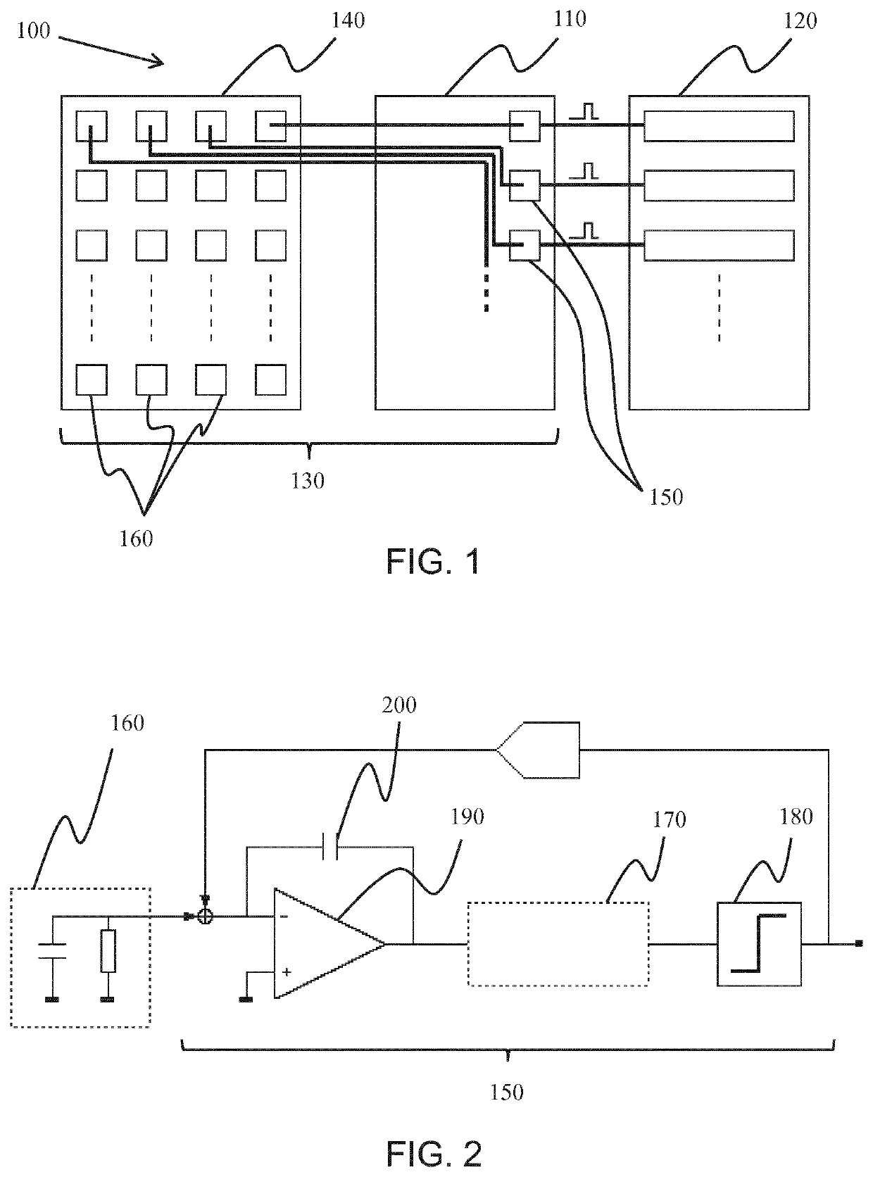
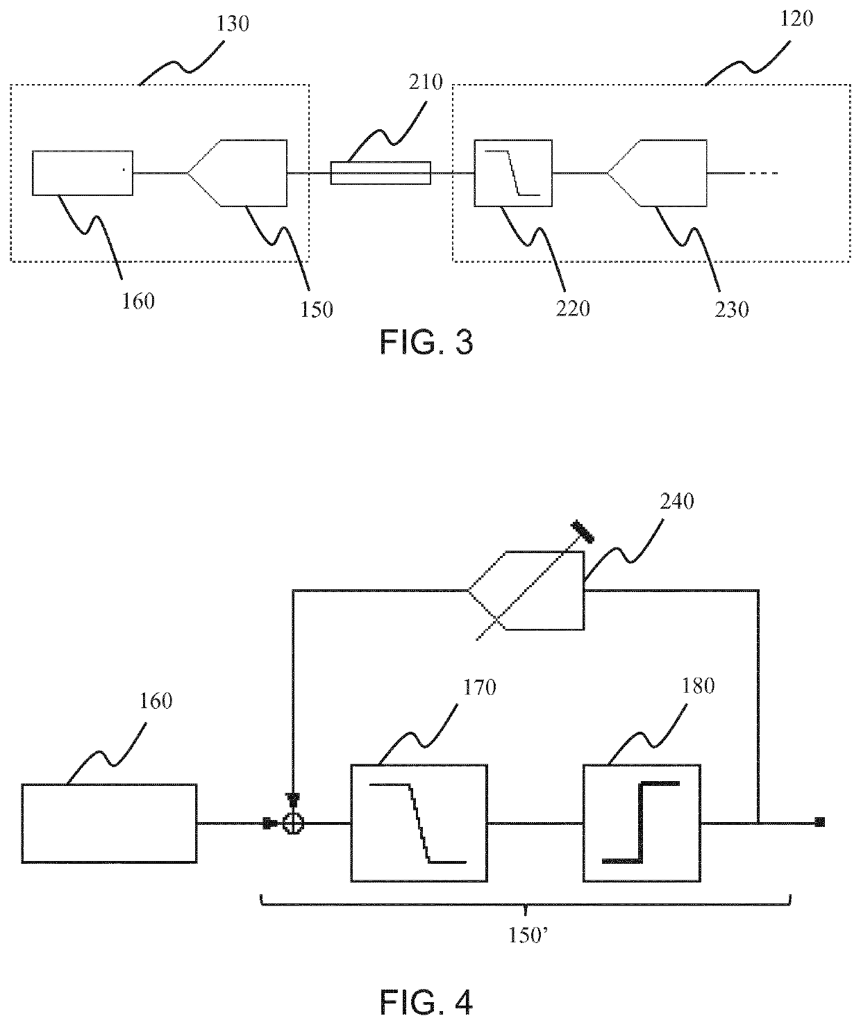
[0237]In a first aspect, there is provided a signal processing system, for transferring analog signals from a probe to a remote processing unit. The system comprises a first ASIC at a probe, which is adapted to receive an analog probe signal. The first ASIC comprises an asynchronous sigma-delta modulator, wherein the asynchronous sigma-delta modulator is adapted to: receive the analog probe signal; and output a binary bit-stream. The system further comprises a second ASIC at the remote processing unit, adapted to receive the binary bit-stream.

[0238]FIG. 1 shows a schematic of the signal processing system 100. The signal processing system comprises a first ASIC 110 and a second ASIC 120, with the first ASIC located on a probe 130 and the second ASIC located on a remote processing unit.

[0239]In the example shown in FIG. 1, the signal processing system forms part of an ultrasound system, wherein the probe 130, housing the first ASIC 110, further includes an acoustic transducer array 14...


PUM


Abstract

The invention provides a signal processing system, for transferring analog signals from a probe to a remote processing unit. The system comprises a first ASIC at a probe, which is adapted to receive an analog probe signal. The first ASIC comprises an asynchronous sigma-delta modulator, wherein the asynchronous sigma-delta modulator is adapted to: receive the analog probe signal; and output a binary bit-stream. The system further comprises a second ASIC at the remote processing unit, adapted to receive the binary bit-stream. The asynchronous may further include a time gain function circuit, the first ASIC may further comprise a multiplexer, the second ASIC may further comprise a time-to-digital converter. The time to digital converter may be a pipelined time-to-digital converter.

Description

FIELD OF THE INVENTION[0001]This invention relates to the field of signal processing, and more specifically to the field of signal processing across multiple, spatially separated stages within an ultrasound system.BACKGROUND OF THE INVENTION[0002]In the construction of an ultrasound probe, high voltage technologies are required to drive the acoustic transducer elements and amplify the received signals. However, these high voltage technologies are not suitable for the implementation of more complex functions, such as analog-to-digital conversion (ADC) and digital signal processing (DSP), simply due to the large feature size of the transistors in these technology nodes, which leads to prohibitively high area, and power, consumption and low speed. This issue drives system choices toward the high voltage integrated circuit containing a minimal functionality that is sufficient to transport the signal to a separate low voltage integrated circuit capable of performing the required signal p...

Claims


Application Information

Patent Timeline
IPC IPC(8): H03M3/00A61B8/08H03M1/12H03M1/50
CPCH03M3/30H03M1/50H03M1/125A61B8/5207A61B8/00H03M1/123H03M1/164H03M3/466
Inventor OUZOUNOV, SOTIR FILIPOVTOTEV, EMIL DIMITROV
Owner KONINKLJIJKE PHILIPS NV
Learn More