Power amplifier circuit
- Summary
- Abstract
- Description
- Claims
- Application Information
AI Technical Summary
Benefits of technology
Problems solved by technology
Method used
Image
Examples
first embodiment
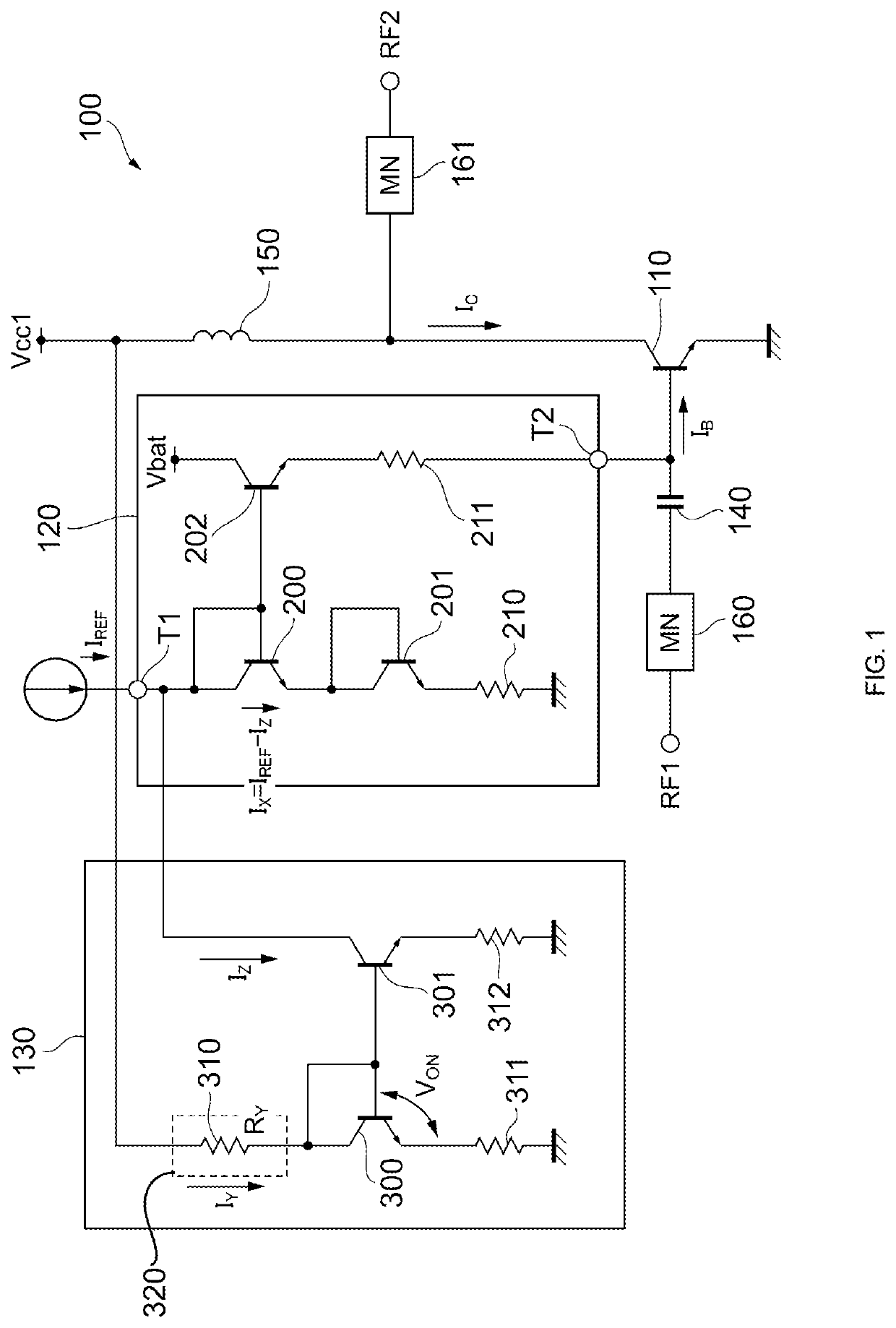
[0022]FIG. 1 illustrates an example configuration of a power amplifier circuit 100 according to the present disclosure. The power amplifier circuit 100 is mounted in, for example, a mobile communication device such as a mobile phone and is used to amplify power of a radio-frequency (RF) signal to be transmitted to a base station. For example, the power amplifier circuit 100 amplifies transmission signals conforming to communication standards such as the second-generation mobile communication system (2G), the third-generation mobile communication system (3G), the fourth-generation mobile communication system (4G), the fifth-generation mobile communication system (5G), Long Term Evolution Frequency Division Duplex (LTE-FDD), LTE Time Division Duplex (LTE-TDD), LTE-Advanced, and LTE-Advanced Pro. The RF signal has a frequency of about several hundreds of megahertz (MHz) to about several tens of gigahertz (GHz), for example. The power amplifier circuit 100 may amplify signals having oth...
second embodiment
[0062]FIG. 4 illustrates an example configuration of a power amplifier circuit 100B according to the present disclosure. As illustrated in FIG. 4, compared to the power amplifier circuit 100, the power amplifier circuit 100B includes a regulation circuit 130A in place of the regulation circuit 130.
[0063]Compared to the regulation circuit 130, the regulation circuit 130A includes a variable resistor circuit 330 whose resistance value is adjustable, in place of the resistance element 310. The variable resistor circuit 330 is a specific example of a current output circuit that converts the power supply voltage Vcc1 into a current and outputs the current. Specifically, the variable resistor circuit 330 includes three resistance elements 340a to 340c and three switches 350a to 350c. The three resistance elements and three switches are for illustrative purposes only, and the number of resistance elements and the number of switches are not limited to those illustrated in FIG. 4.
[0064]The t...
third embodiment
[0069]FIG. 5 illustrates an example configuration of a power amplifier circuit 100C according to the present disclosure. As illustrated in FIG. 5, compared to the power amplifier circuit 100, the power amplifier circuit 100C further includes a capacitor 141.
[0070]The capacitor 141 is disposed between the base and collector of the transistor 110. The functions of the capacitor 141 will now be described with reference to FIGS. 6 and 7.
[0071]FIG. 6 illustrates an equivalent circuit of a transistor. In FIG. 6, the resistance value of the base is denoted by rB, the resistance value of the collector is denoted by rC, the resistance value of the input impedance of the transistor is denoted by rπ, the transconductance is denoted by gm, the capacitance value of the parasitic capacitance between the base and emitter is denoted by CBE, the capacitance value of the parasitic capacitance between the base and collector is denoted by CBC, and the inductance value of the parasitic inductance betwee...
PUM
 Abstract
Description
Claims
Application Information
 - R&D
- Intellectual Property
- Life Sciences
- Materials
- Tech Scout
- Unparalleled Data Quality
- Higher Quality Content
- 60% Fewer Hallucinations
Browse by: Latest US Patents, China's latest patents, Technical Efficacy Thesaurus, Application Domain, Technology Topic, Popular Technical Reports.
© 2025 PatSnap. All rights reserved.Legal|Privacy policy|Modern Slavery Act Transparency Statement|Sitemap|About US| Contact US: help@patsnap.com


