
Garbage collection in non-volatile memory that fully programs dependent layers in a target block

a non-volatile memory and target block technology, applied in the field of data processing and data storage, can solve the problems of reducing the reliability, endurance, and latency of nand flash memory, and the page of the same page, so as to reduce the overprovisioning, increase the bit error rate, and reduce the storage capacity.

Active Publication Date: 2020-08-13
IBM CORP
View PDF3 Cites 13 Cited by
  • Summary
  • Abstract
  • Description
  • Claims
  • Application Information

AI Technical Summary

Benefits of technology

The patent text discusses a problem in NAND flash memory where increasing the storage capacity has led to reduced reliability and increased latency. This is due to factors like data retention, program disturb, and read disturb effects. To address this, read threshold voltage calibration is commonly employed, but this can result in bit error rates that are uncorrectable through error correction codes. The patent proposes a solution by fully programming a dependent layer in a target block during garbage collection to avoid leaving an open interface. This improves read threshold voltage calibration and reduces the likelihood of bit errors.

Problems solved by technology

This desirable trend of increasing storage density has unfortunately led to reductions in the reliability, endurance, and latency of NAND flash memory.
Consequently, if pages of the same page group have different retention times, all pages in the page group will likely experience sub-optimal read threshold voltage calibration (and a higher bit error rate).
In other implementations in which only a subset of pages or a single page of the page group is used for read threshold voltage calibration, any page of the same page group having a different data retention time than the page(s) used for read threshold voltage calibration will experience a significantly higher bit error rate.
Consequently, a read retry or error recovery procedure may be required to read the data of the page, resulting in a significant increase in read latency and / or an uncorrectable read error.
Another phenomenon that has been observed in NAND flash memory employing multi-bit cells (e.g., MLC, TLC, and / or QLC) is an increase in the bit error rate in pages having an “open interface,” that is, pages for which adjacent word lines and / or word-layers have not been programmed yet, for example, as result of a vendor-specific page programming order.
However, because some word lines will remain partially programmed with synthetic data, writes to these word lines after the programming pause will still result in cell-to-cell interference to the previously programmed layer.
Further, programming of synthetic data—especially if done frequently—wastes storage capacity, artificially reduces the overprovisioning, and thereby increases write amplification.

Method used


Image

  • Garbage collection in non-volatile memory that fully programs dependent layers in a target block
  • Garbage collection in non-volatile memory that fully programs dependent layers in a target block
  • Garbage collection in non-volatile memory that fully programs dependent layers in a target block

Examples


Embodiment Construction

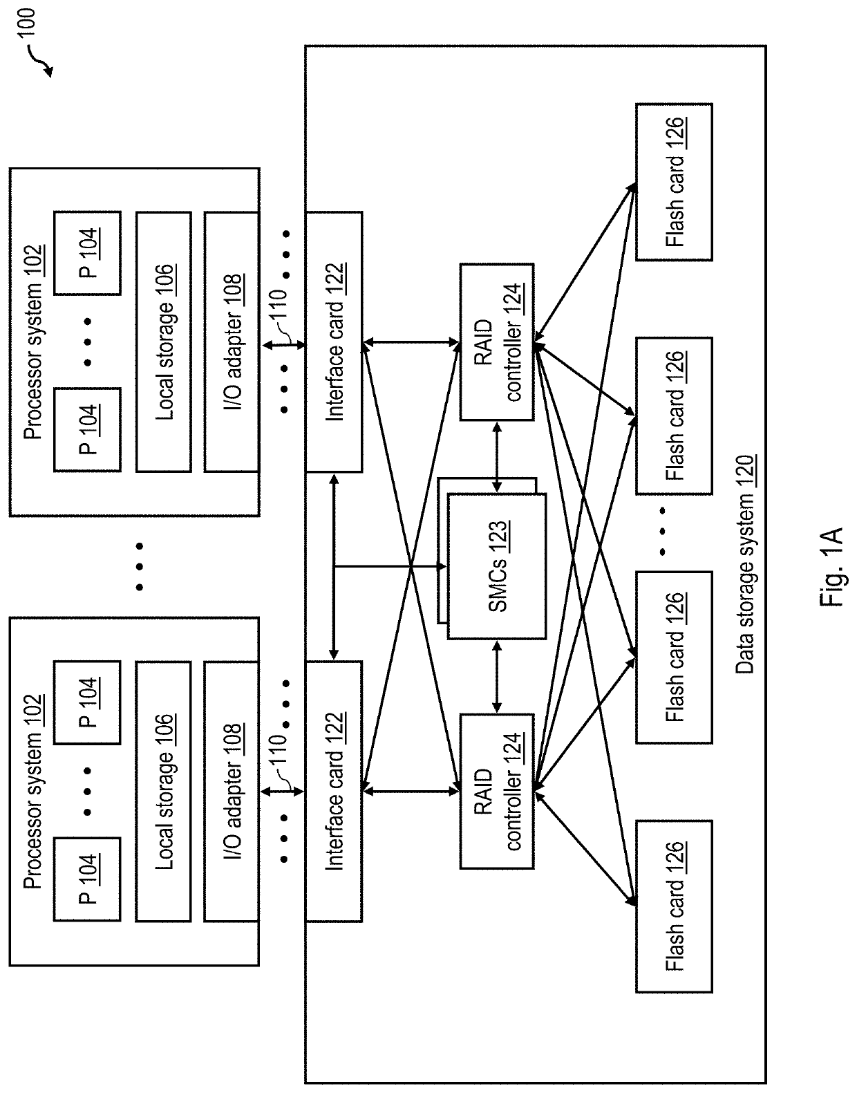
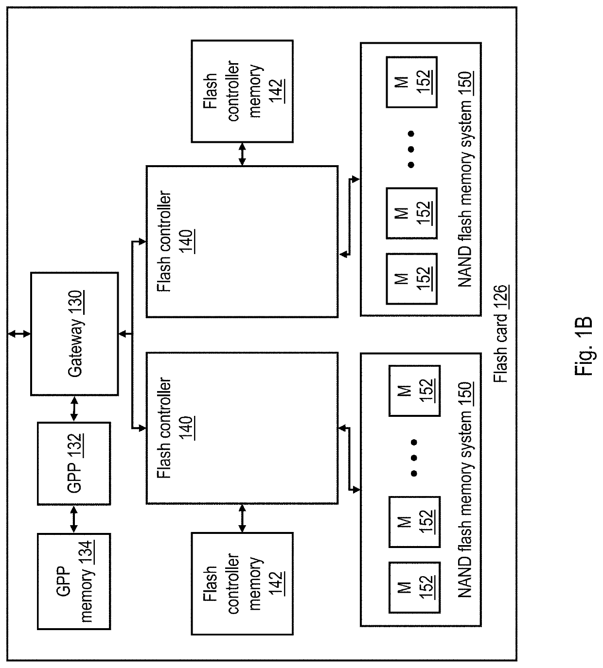
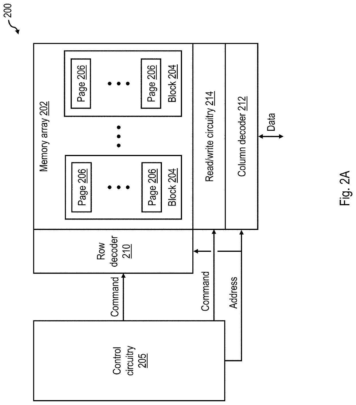
[0017]With reference to the figures and with particular reference to FIG. 1A, there is illustrated a high level block diagram of an exemplary data processing environment 100 including a data storage system 120 having a non-volatile memory array as described further herein. As shown, data processing environment 100 includes one or more hosts, such as a processor system 102 having one or more processors 104 that process instructions and data. A processor system 102 may additionally include local storage 106 (e.g., dynamic random access memory (DRAM) or disks) that may store program code, operands and / or execution results of the processing performed by processor(s) 104. In various embodiments, a processor system 102 can be, for example, a mobile computing device (such as a smartphone or tablet), a laptop or desktop personal computer system, a server computer system (such as one of the POWER series of servers available from International Business Machines Corporation), or a mainframe co...


PUM


Abstract

A non-volatile memory includes a plurality of blocks of physical memory, including a target block and at least one source block containing at least some valid data and some invalid data. Responsive to determining to perform garbage collection for the non-volatile memory, the controller transfers valid data from the at least one source block to the target block. The controller ends garbage collection on the at least one source block with at least some valid data present in the at least one source block and all interfaces of the target block closed at the boundary of independent layers. In at least some embodiments, the target block may be configured to store more bits per cell than the at least one source block.

Description

BACKGROUND OF THE INVENTION[0001]This disclosure relates to data processing and data storage, and more specifically, to garbage collection in a non-volatile memory system. Still more particularly, the disclosure relates to techniques for garbage collection in a non-volatile memory system that fully program dependent layers in a target block.[0002]NAND flash memory is an electrically programmable and erasable non-volatile memory technology that stores one or more bits of data per memory cell as a charge on the floating gate of a transistor or a similar charge trap structure. The amount of charge on the floating gate modulates the threshold voltage of the transistor. By applying a proper read voltage and measuring the amount of current, the programmed threshold voltage of the memory cell can be determined and thus the stored information can be detected. Memories storing one, two, three and four bits per cell are respectively referred to in the art as Single Level Cell (SLC), Multi-Lev...

Claims


Application Information

Patent Timeline
IPC IPC(8): G06F12/02G06F3/06
CPCG06F2212/7205G06F12/0253G06F3/0679G06F12/0246G06F3/0608G06F3/0652G06F3/0647G06F3/0688G06F2212/1044G06F2212/7201
Inventor PLETKA, ROMAN A.PAPANDREOU, NIKOLAOSTOMIC, SASAIOANNOU, NIKOLASFRY, AARON D.FISHER, TIMOTHY
Owner IBM CORP
Learn More