Patterning of nanostructures using imprint lithography

Pending Publication Date: 2019-08-08
UNIV OF MASSACHUSETTS
View PDF0 Cites 5 Cited by
  • Summary
  • Abstract
  • Description
  • Claims
  • Application Information

AI Technical Summary

Benefits of technology

The patent describes a method for creating membranes with high aspect ratio crystalline inorganic oxide nanostructures using a soft nanoimprint lithography technique. The method involves inking metal oxide nanoparticles and creating nanopatterns with low-shrinkage at high temperatures. The nanopatterns have good porosity and can be used for creating complex 2-D and 3-D nanostructures without the need for conventional subtractive processing steps. The invention allows for rapid and efficient preparation of crystalline metal oxide nanostructures with high integration density.

Problems solved by technology

Consequently, patterned inorganic film fabrication is often cost, equipment, materials and energy intensive and is not amendable to continuous as opposed to batch fabrication.
Among the most significant challenges are fabrication rate and integration density.
While an effective additive approach, challenges for DIW include rate limitations due to serial writing and direct printing of deep sub-micron features without relying on volumetric shrinkage of precursor structures.
High temperature calcination to obtain a crystalline phase is accompanied by additional reductions in dimensions (60-80%), which causes further dimensional instability and cracking.

Method used


Image

  • Patterning of nanostructures using imprint lithography
  • Patterning of nanostructures using imprint lithography
  • Patterning of nanostructures using imprint lithography

Examples


examples

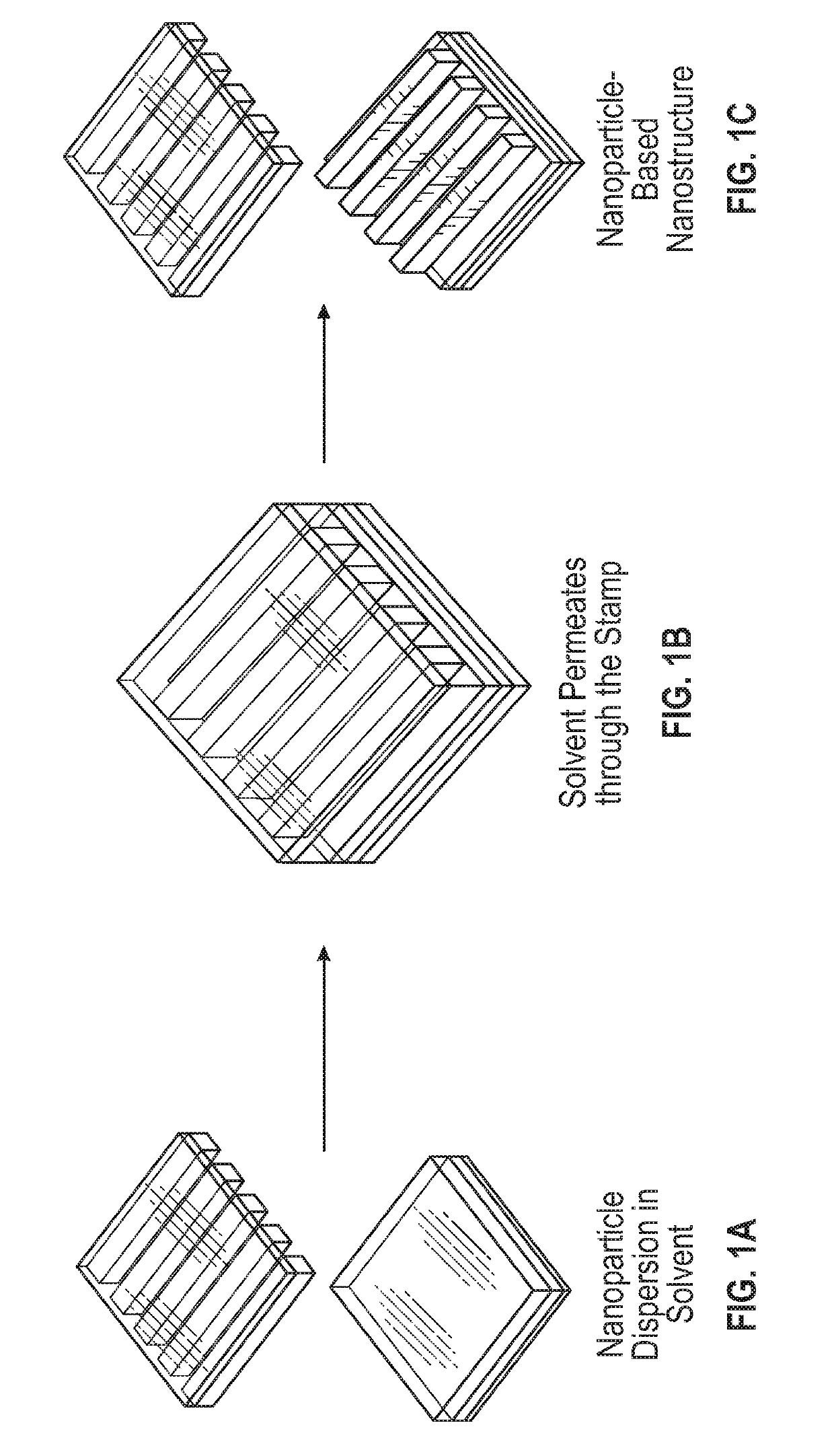
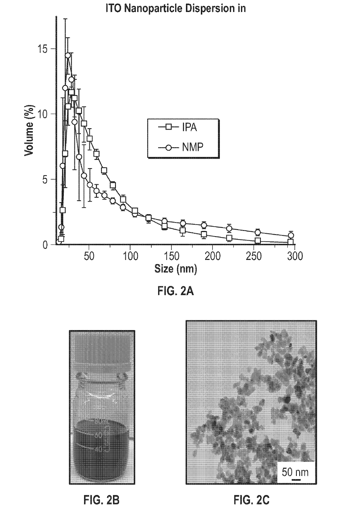
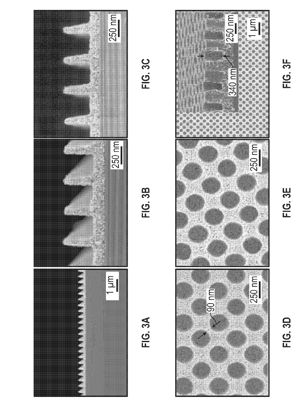
[0078]Various embodiments of the present invention can be better understood by reference to the following Examples which are offered by way of illustration. The present invention is not limited to the Examples given herein.

Fabrication of PDMS Stamps.

[0079]Patterned PDMS stamps were made by casting PDMS against silicon master molds. The silicon masters were cleaned in concentrated sulfuric acid and followed by treating for 15 minutes in an oxygen plasma cleaner. The silicon masters were then placed in a degassed glass jar at 80° C., to which 1 vol % of heptadecafluoro-1,1,2,2-tetrahydrodecyl)dimethylchlorosilane (Gelest Corp.) is introduced for a 12 h period. In this process a self-assembled monolayer of a long chain fluorinated alkane is created on silicon master molds which reduces their surface energy and facilitates easy removal of cured PDMS stamps casted against them in the next step.

[0080]Sylgard 184 silicone elastomer kits (Ellsworth Adhesive) were used to make PDMS stamps fr...


PUM

PropertyMeasurementUnit
Temperatureaaaaaaaaaa
Timeaaaaaaaaaa

Abstract

Various embodiments disclosed relate to methods of manufacturing a textured surface comprising disposing a nanoparticulate ink on a substrate.

Description

CROSS-REFERENCE TO RELATED APPLICATION[0001]This application claims the benefit of priority to U.S. Provisional Patent Application Ser. No. 62 / 359,967 entitled “DIRECT PATTERNING OF OXIDE NANOSTRUCTURES USING IMPRINT LITHOGRAPHY AND NANOPARTICLE DISPERSION INKS,” filed Jul. 8, 2016, the disclosure of which is incorporated herein in its entirety by reference.STATEMENT OF GOVERNMENT SUPPORT[0002]This invention was made with Government support under Nos. CMMI-1025020 and CMMI-1258336 awarded by National Science Foundation. The U.S. Government has certain rights in this invention.BACKGROUND[0003]Patterned metal oxide and semiconductor films are ubiquitous in functional device architectures. Typical fabrication pathways are subtractive by nature and contain multiple steps, including deposition of a planar film by chemical or physical deposition methods such sputtering or chemical vapor deposition, application of a photoresist, patterning of the resist using optical lithography, developme...

Claims


Application Information

Patent Timeline
IPC IPC(8): G03F7/00B29C71/02C09D11/52C09D11/037C09D11/033
CPCG03F7/0002B29C71/02C09D11/52C09D11/037C09D11/033B29C2071/022B32B5/16B32B5/30B32B3/10C23C18/06C23C18/1254C23C18/1283G03F1/00H01L21/02288
Inventor WATKINS, JAMES J.KOTHARI, ROHIT
Owner UNIV OF MASSACHUSETTS
Why Eureka
Try Eureka