Semiconductor device

Inactive Publication Date: 2019-07-11
MITSUBISHI ELECTRIC CORP
View PDF1 Cites 0 Cited by
  • Summary
  • Abstract
  • Description
  • Claims
  • Application Information

AI Technical Summary

Benefits of technology

The semiconductor device in this patent is designed to prevent damage during the manufacturing process. It includes a layer of silicon oxide with an opening for a copper electrode, a layer of copper placed on top of the silicon oxide layer, and a layer of a material with higher fracture toughness than the silicon oxide layer. This helps to absorb impacts and relieve stress during the process, reducing the risk of defects in the semiconductor device.

Problems solved by technology

A surface electrode mainly composed of aluminum (Al) is used for a semiconductor element operating at less than 200° C., an Al wire is bonded to the surface electrode, and when such semiconductor elements are operated at a temperature exceeding 200° C., there is a problem that the shape of the surface electrode and the wire are changed and reliability thereof is lowered.
However, as compared with an Al wire, a Cu wire has a large impact on an element when bonding to the surface electrode, therefore, there is a problem of element defect.

Method used


Image

  • Semiconductor device
  • Semiconductor device
  • Semiconductor device

Examples


embodiment 1

A. Embodiment 1

[0019]

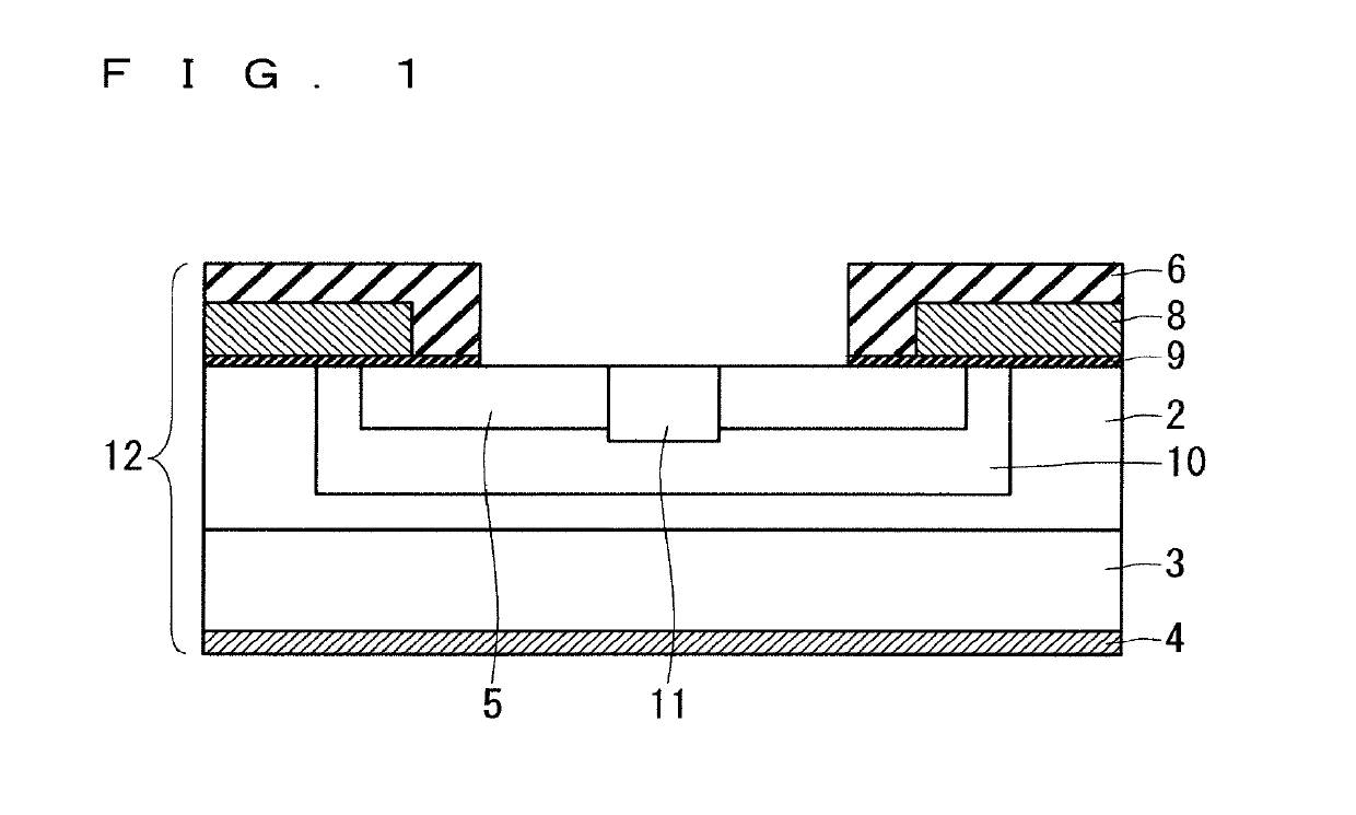
[0020]FIG. 1 is a cross-sectional view illustrating a configuration of a power semiconductor element according to Embodiment 1. Hereinafter, the configuration of the power semiconductor element 12 will be described. For a substrate of the power semiconductor element 12, a SiC substrate 3 is used, and an element structure is formed thereon. If the SiC substrate is used, a low-loss semiconductor element capable of a high speed operation and a high-temperature operation as compared with the conventionally used Si substrate can be fabricated. In FIG. 1, the power semiconductor element 12 is shown as a Metal-Oxide-Semiconductor Field-Effect-Transistor (MOSFET).

[0021]On the surface side of the SiC substrate 3, a drift layer 2 is formed by epitaxial growth, and a rear surface electrode 4 electrically connected to the SiC substrate 3 is formed on the rear surface side thereof. On the surface layer of the drift layer 2, a base region 10 is partially formed, and a source ...

embodiment 2

B. Embodiment 2

[0044]

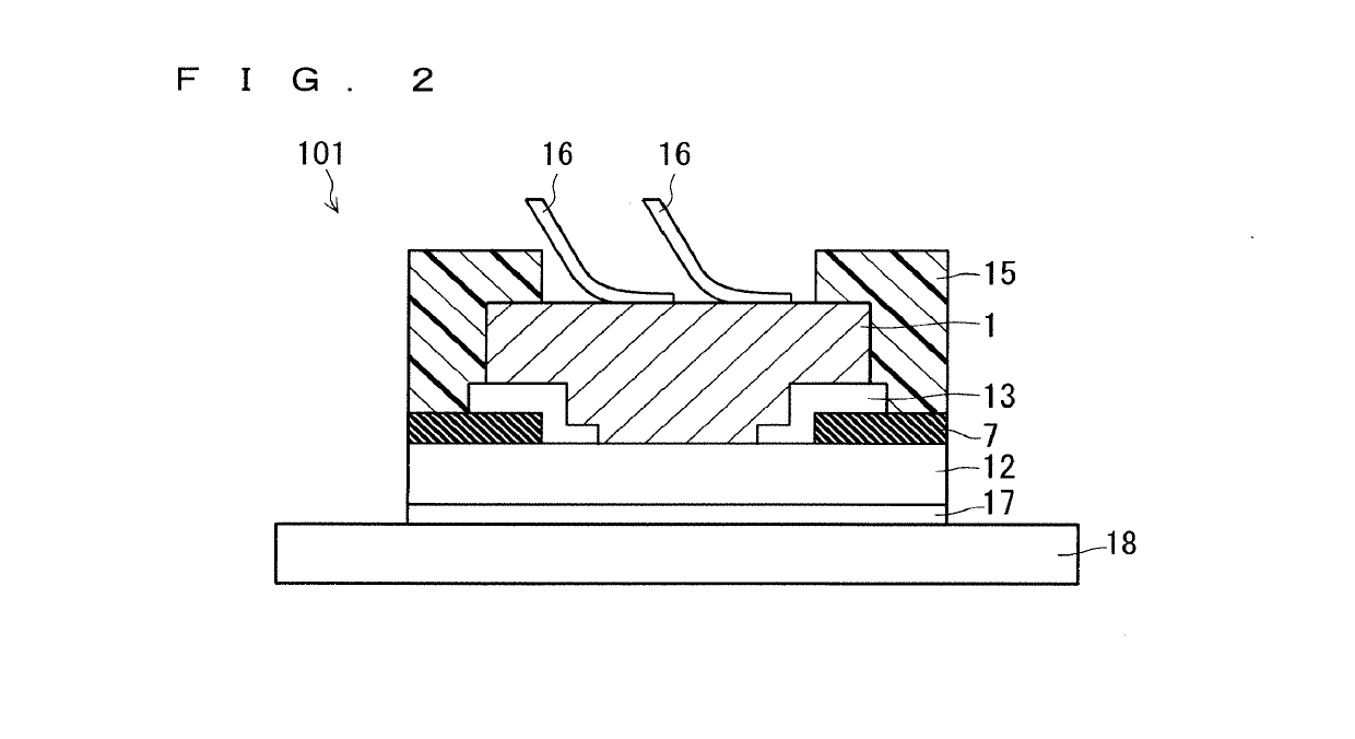
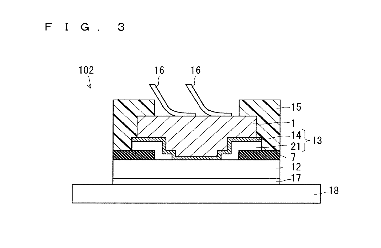
[0045]FIG. 4 is a cross-sectional view illustrating a configuration of a semiconductor device 103 according to Embodiment 2. The semiconductor device 103 is similar to the semiconductor device 102 in that a part of the stress relieving layer 13 is formed of the barrier metal layer 14 having a higher fracture toughness value than the interlayer insulating film 7 made of SiO2, however, the semiconductor device 103 differs from the semiconductor device 102 in that the barrier metal layer 14 is provided between the interlayer insulating film 7 and the non-barrier metal stress relieving layer 21. Apart from the above, the configuration of the semiconductor device 103 is similar to that of the semiconductor device 102.

[0046]In the semiconductor device 102, the barrier metal layer 14 is provided between the Cu electrode 1 and the non-barrier metal stress relieving layer 21 so that Cu of the Cu electrode does not diffuse in the stress relieving layer 13. However, when t...

embodiment 3

C. Embodiment 3

[0051]

[0052]FIG. 5 is a cross-sectional view illustrating a configuration of a semiconductor device 104 according to Embodiment 3. In Embodiment 1 and Embodiment 2, the stress relieving layer 13 has an opening portion on the opening portion of the interlayer insulating film 7, and the Cu electrode 1 and the source region 5 of the power semiconductor element 12 are electrically connected through the opening portion of the stress relieving layer 13. Meanwhile, in Embodiment 3, the configuration is that the stress relieving layer 13 is formed all over the lower side of Cu electrode 1, over from the opening portion of the interlayer insulating film 7 to above the interlayer insulating film 7. Even with such a structure, by forming the stress relieving layer 13 with an electric conductor, the Cu electrode 1 electrically connected to the source region 5 of the power semiconductor element 12 at the opening portion of the interlayer insulating film 7, through the stress relie...


PUM


Abstract

The object of the present invention is to suppress cracks in the interlayer insulating film attributed to growth of Cu crystal grains. The semiconductor device (101) includes a source region (5), an interlayer insulating film (7) made of silicon oxide, having an opening portion, and formed on the source region (5), a Cu electrode (1) electrically connected to the source region (5) through the opening portion of the interlayer insulating film (7) and an end portion thereof is located on the interlayer insulating film (7) inside an end portion of the interlayer insulating film (7), and a stress relieving layer (13) formed between the Cu electrode (1) and the interlayer insulating film (7), made of a material having a higher fracture toughness value than the interlayer insulating film (7), and extending from the inside to the outside of the end portion of the Cu electrode (1).

Description

TECHNICAL FIELD[0001]The present invention relates to a structure for relieving an impact during wire bonding of a semiconductor device.BACKGROUND ART[0002]Silicon carbide (SiC) has a larger band gap than silicon (Si). Therefore, a semiconductor element using SiC can operate at a higher temperature than a semiconductor element using Si which operates at less than 200° C.[0003]A surface electrode mainly composed of aluminum (Al) is used for a semiconductor element operating at less than 200° C., an Al wire is bonded to the surface electrode, and when such semiconductor elements are operated at a temperature exceeding 200° C., there is a problem that the shape of the surface electrode and the wire are changed and reliability thereof is lowered. Therefore, copper (Cu) with high reliability at high temperature has been studied as a material of the surface electrode and the wire in place of Al.[0004]However, as compared with an Al wire, a Cu wire has a large impact on an element when bon...

Claims


Application Information

Patent Timeline
IPC IPC(8): H01L21/3205H01L21/768H01L23/532
CPCH01L21/32051H01L21/768H01L23/5329H01L2224/4847H01L2224/4911H01L2224/05147H01L21/3205H01L23/522H01L2224/05H01L2224/02166H01L24/05H01L2224/04042H01L2924/00014H01L29/1608H01L2924/00H01L24/45H01L2924/10272H01L2224/48463H01L2924/13055H01L2224/45147
Inventor SUZUKI, HIROYOSHIOKABE, HIROAKI
Owner MITSUBISHI ELECTRIC CORP
Why Eureka
Try Eureka