Semiconductor device with photonic and electronic functionality and method for manufacturing a semiconductor device

a semiconductor device and electronic functionality technology, applied in the field of photonics and photonic chips, can solve the problems of parasitic capacitance and resistance, limited stack density of optical and electrical components, and reduced signal transfer speed, and achieve the effect of increasing the stack density of optical and increasing the speed of signal transfer

Active Publication Date: 2019-01-24
AMS AG
View PDF9 Cites 5 Cited by
  • Summary
  • Abstract
  • Description
  • Claims
  • Application Information

AI Technical Summary

Benefits of technology

[0005]The present disclosure provides an improved concept for semiconductor devices with photonic and electronic functionality that allows for a higher stack density of optical and electronic, in particular active electronic, components and an increased speed of signal transfer.

Problems solved by technology

However, such approaches may be limited in stack density of optical and electrical components and / or may suffer from parasitic capacitances and resistances.
This may also result in a reduced speed of signal transfer.

Method used


Image

  • Semiconductor device with photonic and electronic functionality and method for manufacturing a semiconductor device
  • Semiconductor device with photonic and electronic functionality and method for manufacturing a semiconductor device
  • Semiconductor device with photonic and electronic functionality and method for manufacturing a semiconductor device

Examples


Embodiment Construction

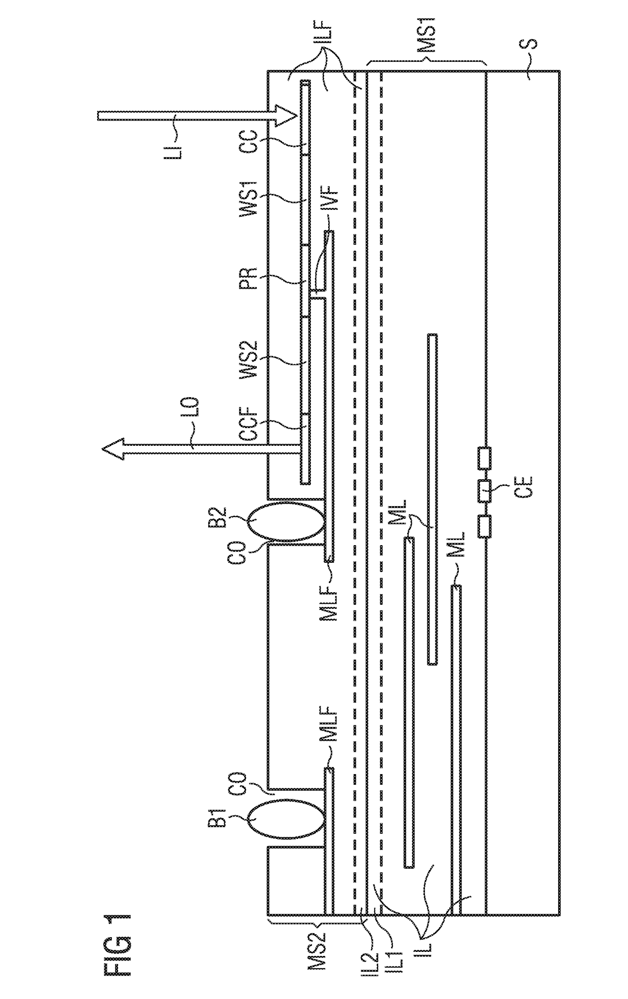
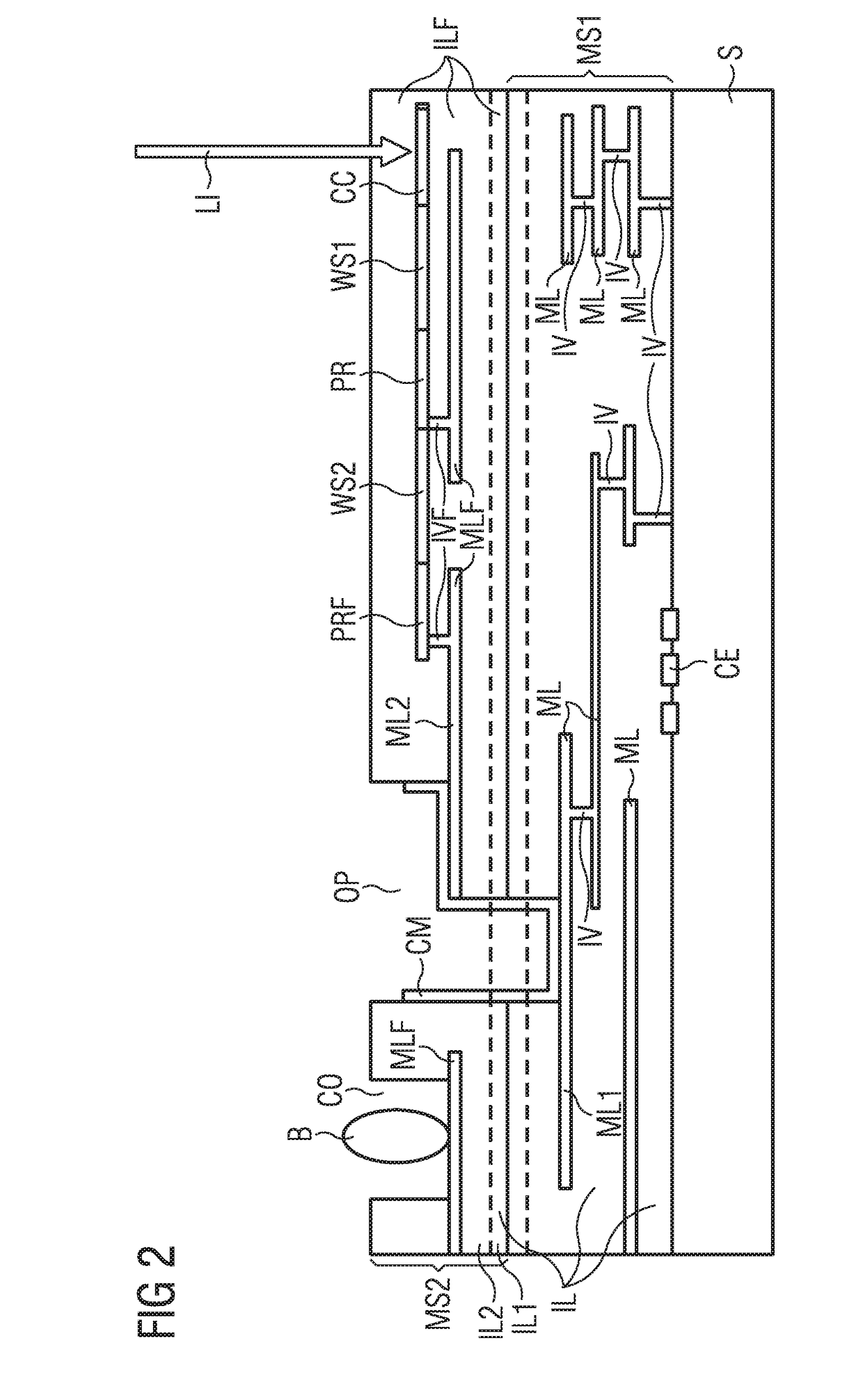
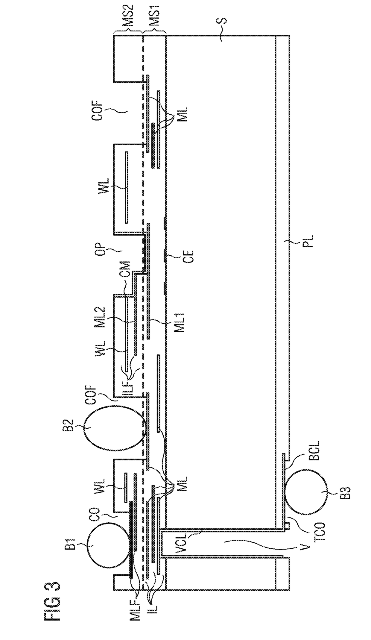
[0084]FIG. 1 shows an exemplary implementation of a semiconductor device according to the improved concept.

[0085]The semiconductor device comprises a semiconductor substrate S, a first metallization stack MS1 arranged on the semiconductor substrate S and a second metallization stack MS2 arranged on the first metallization stack MS1, in particular on a side of the first metallization stack MS1 facing away from the substrate S.

[0086]The substrate S comprises or carries a plurality of circuit elements CE, wherein the circuit elements CE comprise active electronic components, for example transistor circuitry. The circuit elements CE and the active electronic components may for example be implemented according to a CMOS technology.

[0087]The first metallization stack MS1 comprises electrically insulating layers IL and metallization layers ML. It is pointed out that the metallization layers ML are depicted only schematically in FIG. 1. In particular, the metallization layers ML may establi...


PUM


Abstract

A semiconductor device has a semiconductor substrate and a first metallization stack arranged on the substrate. The substrate has and/or carries a plurality of electronic circuit elements. The first metallization stack has electrically insulating layers and at least one metallization layer. The semiconductor device further has a second metallization stack arranged on the first metallization stack and comprising further electrically insulating layers and an optical waveguide layer. The optical waveguide layer has at least one optical waveguide structure. Furthermore, one of the electrically insulating layers and one of the further electrically insulating layers are in direct contact with each other and form a pair of directly bonded layers.

Description

BACKGROUND OF THE INVENTION[0001]The present disclosure relates to the field of photonics and photonic chips. In particular, the present disclosure relates to a semiconductor device with photonic and electronic functionality and to a method for manufacturing a semiconductor device with photonic and electronic functionality.[0002]In the field of photonics, there is a trend from long-distance signal transfer via optical fibers towards optical signal processing on-board and / or on-chip. For on-chip processing of optical signals, it may be important to have a dense stack of optical and electrical components, that is a dense stack of components with photonic functionality and electronic functionality, in particular active electronic functionality.[0003]For example CMOS integrated circuit chips may be mounted on a silicon-on-insulator wafer comprising optical waveguides by means of metal pads and bump bonding and / or wire bonding techniques.[0004]However, such approaches may be limited in s...

Claims


Application Information

Patent Timeline
Patent Type & Authority Applications(United States)
IPC IPC(8): G02B6/12H01L23/522H01L21/48H01L23/00G02B6/13
CPCG02B6/12004H01L23/5226H01L21/4857H01L24/89H01L24/08G02B6/13H01L2224/80896H01L2224/08145G02B2006/12061G02B2006/12107G02B6/428G02B6/34G02B6/4214G02B6/43H01L23/481H04B10/801H01L2224/02371H01L24/05H01L24/06H01L24/13H01L24/14H01L24/16H01L2224/0401H01L2224/05548H01L2224/05567H01L2224/06181H01L2224/131H01L2224/1403H01L2224/14181H01L2224/16145H01L2224/16227H01L2924/014H01L2924/00014
Inventor KRAFT, JOCHENSIEGERT, JOERG
Owner AMS AG
Why Eureka
Try Eureka