Light emitting device, biological information measuring apparatus, and method of manufacturing light emitting device

a technology biological information, applied in the field can solve the problems of complex manufacturing process of light emitting devices, achieve the effect of preventing the area of the reflecting region from being reduced, ensuring the area of the reflecting region withou, and preventing the miniaturization of the light emitting devi

Active Publication Date: 2018-07-12
SEIKO EPSON CORP
View PDF3 Cites 1 Cited by
  • Summary
  • Abstract
  • Description
  • Claims
  • Application Information

AI Technical Summary

Benefits of technology

[0007]In a preferred example of the light emitting device according to the aspect of the invention, the area of the mounting region is greater than the area of the light emitting element by four hundred times or less seen in the direction perpendicular to the wiring substrate. In this configuration, the area of the mounting region is greater than the area of the light emitting element by four hundred times or less seen in the direction perpendicular to the wiring substrate. Therefore, it is possible to sufficiently ensure an area of the reflecting region without hindering miniaturization of the light emitting device.
[0008]In a preferred example of the light emitting device according to the aspect of the invention, the wiring substrate has a hole which is formed within a bonding region of the reflecting electrode where the light emitting element is bonded and into which the bonding material infiltrates. In this configuration, the wiring substrate has the hole which is formed within the bonding region where the light emitting element is bonded and into which the bonding material infiltrates. Therefore, compared to a configuration in which the wiring substrate has no hole which is formed within the bonding region and into which the bonding material infiltrates, the bonding material flowing out of the bonding region can be minimized. Thus, the area of the reflecting region can be prevented from being reduced.
[0009]In a preferred example of the light emitting device according to the aspect of the invention, the hole is formed entirely or partially along the reflecting electrode in a thickness direction. In this configuration, the hole into which the bonding material infiltrates is formed entirely or partially along the reflecting electrode in the thickness direction. Therefore, an influence of the bonding material on the wiring substrate can be minimized.
[0010]A biological information measuring apparatus according to an aspect of the invention includes the various light emitting devices described above. In this configuration, an operation and an effect similar to those of the various light emitting devices described above are achieved.
[0011]A method of manufacturing a light emitting device according to an aspect of the invention includes bonding a light emitting element which emits light and a light reflective reflecting electrode on a wiring substrate, using a bonding material. The reflecting electrode has a reflecting region which reflects light emitted from the light emitting element. An area of a mounting region surrounded by an outer circumference of the reflecting region is greater than an area of the light emitting element by four times or more seen in a direction perpendicular to the wiring substrate. In this method, a light emitting device, in which the light emitting element that emits light and the light reflective reflecting electrode on the wiring substrate are bonded to each other using the bonding material, the reflecting electrode has the reflecting region that reflects light emitted from the light emitting element, and the area of the mounting region surrounded by the outer circumference of the reflecting region is greater than the area of the light emitting element by four times or more seen in the direction perpendicular to the wiring substrate, is manufactured. Therefore, it is possible to manufacture a light emitting device in which the reflecting electrode sufficiently reflects light emitted from the light emitting element even though a reflective film for reflecting light emitted from the light emitting element is not separately provided. Thus, a process of manufacturing a light emitting device is simplified.
[0012]In a preferred example of the method of manufacturing a light emitting device according to the aspect of the invention, the wiring substrate has a hole which is formed within a bonding region where the light emitting element is bonded and into which the bonding material infiltrates. It is preferable that in bonding the light emitting element and the reflecting electrode, the light emitting element and the reflecting electrode are bonded to each other such that the bonding material flows into the hole. In this method, the light emitting element and the reflecting electrode are bonded to each other such that the bonding material flows into the hole which is formed within the bonding region where the light emitting element is bonded and into which the bonding material infiltrates. Therefore, the bonding material flowing out of the bonding region can be minimized. Thus, an area of the reflecting region can be prevented from being reduced.

Problems solved by technology

Accordingly, a process of manufacturing a light emitting device is complicated.

Method used


Image

  • Light emitting device, biological information measuring apparatus, and method of manufacturing light emitting device
  • Light emitting device, biological information measuring apparatus, and method of manufacturing light emitting device
  • Light emitting device, biological information measuring apparatus, and method of manufacturing light emitting device

Examples


first embodiment

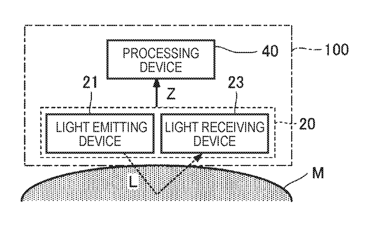
[0025]A biological information measuring apparatus 100 of a first embodiment is a measuring instrument for measuring biological information of a test subject and is mounted on a site (hereinafter, will be referred to as the “measurement site”) M that is a measurement target in the body of the test subject. For example, the measurement site M is a wrist or an ankle. In the first embodiment, a pulse rate of the test subject is illustrated as the biological information.

[0026]FIG. 1 is a view of a configuration focused on a function of the biological information measuring apparatus 100. As illustrated in FIG. 1, the biological information measuring apparatus 100 of the first embodiment includes a detecting device 20 and a processing device 40. The detecting device 20 is a sensor module generating a detection signal Z in accordance with the state of the measurement site M. The detecting device 20 of the first embodiment generates the detection signal Z to be used for specifying the pulse...

second embodiment

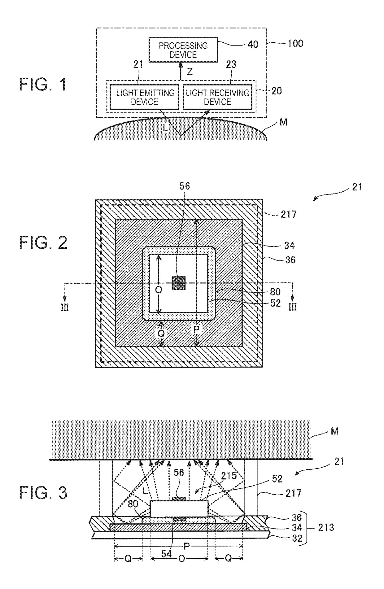
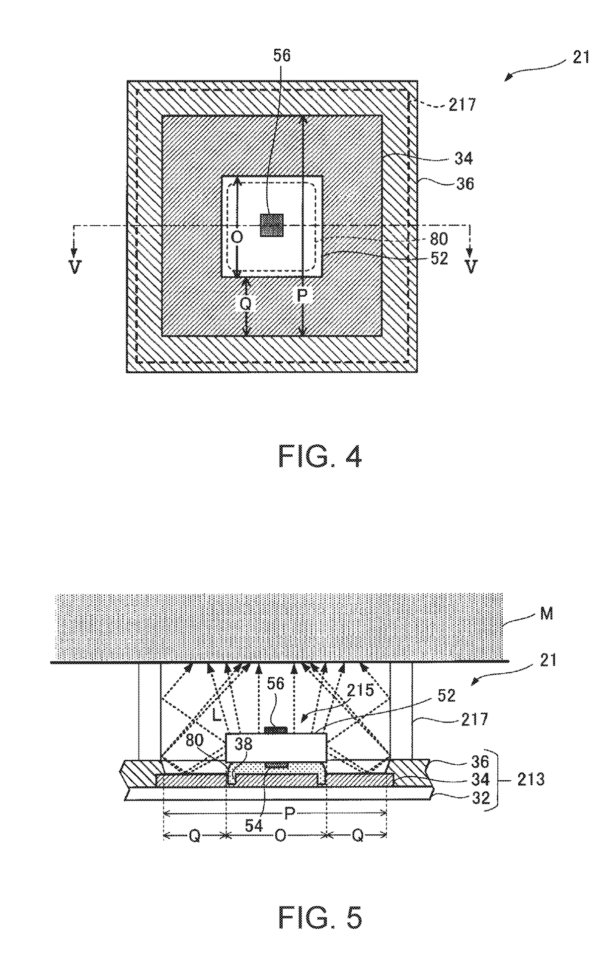
[0037]FIG. 4 is a plan view of a light emitting device 21 according to the second embodiment, and FIG. 5 is a cross-sectional view taken along line V-V in FIG. 4. As illustrated in FIG. 5, similar to the first embodiment, the light emitting device 21 of the second embodiment includes the wiring substrate 213, the light emitting element 215, and the partition wall 217. However, the wiring substrate 213 of the second embodiment has holes 38 in which the bonding material 80 infiltrates.

[0038]FIG. 6 is a plan view of the base material 32 before the light emitting element 215 is bonded. As illustrated in FIG. 6, the holes 38 are formed within the bonding region O. In the second embodiment, four holes 38 are formed within the bonding region O. Specifically, the holes 38 form a rectangular shape having each thereof along a side the outer circumference of the bonding region O. In order to maintain the reflecting electrode 34 and the light emitting element 215 being electrically connected to...

modification examples

[0042]Each of the embodiments illustrated above can be variously deformed. Forms of specific deformation will be illustrated below. It is also possible to appropriately combine two or more forms which are arbitrarily selected from the examples below.

[0043](1) In each of the embodiments described above, the area of the mounting region P is greater than the area of the light emitting element 215 by four times seen in the direction perpendicular to the wiring substrate 213. However, the area of the mounting region P is arbitrary as long as the area of the mounting region P is greater than the area of the light emitting element 215 by four times or more seen in the direction perpendicular to the wiring substrate 213. For example, it is possible to preferably employ a configuration in which the area of the mounting region P is greater than the area of the light emitting element 215 by nine times or more seen in the direction perpendicular to the wiring substrate 213. However, from the vi...


PUM


Abstract

A light emitting device includes a light emitting element that emits light, and a wiring substrate that includes a light reflective reflecting electrode to which the light emitting element is bonded using a bonding material. The reflecting electrode has a reflecting region which reflects light emitted from the light emitting element. An area of a mounting region surrounded by an outer circumference of the reflecting region is greater than an area of the light emitting element by four times or more seen in a direction perpendicular to the wiring substrate.

Description

BACKGROUND1. Technical Field[0001]The present invention relates to a light emitting device which emits light.2. Related Art[0002]In the related art, a technology related to a light emitting device which emits light is proposed. For example, JP-A-2008-198962 discloses a light emitting device in which light emitted by a light emitting element bonded to a substrate is concentrated.[0003]According to the technology in JP-A-2008-198962, light emitted by the light emitting element is concentrated using a reflective film formed on the substrate. However, according to the technology in JP-A-2008-198962, the reflective film is formed such that the light emitting element is bonded to a mounting portion on the substrate using a die bond material, and then the die bond material and the mounting portion are covered. Accordingly, a process of manufacturing a light emitting device is complicated.SUMMARY[0004]An advantage of some aspects of the invention is that a process of manufacturing a light e...

Claims


Application Information

Patent Timeline
Patent Type & Authority Applications(United States)
IPC IPC(8): A61B5/024H01L31/173H01L31/02H01L33/60H01L33/62
CPCA61B5/02427H01L31/173H01L31/02019H01L33/60H01L33/62H01L2933/0066H01L2933/0058A61B2562/0238H01L25/167H01L31/167
Inventor KOIKE, SHIGEMITSU
Owner SEIKO EPSON CORP
Why Eureka
Try Eureka