Sputtering cathode, sputtering device, and method for producing film-formed body

a sputtering cathode and film-forming technology, applied in the direction of plasma technique, light and heating apparatus, laminated elements, etc., can solve the problems of difficult film-forming on a flat boardlike body, inability to achieve a sufficiently high deposition rate, and low plasma density between the facing two targets, so as to reduce the risk of body damage, increase plasma density, and high deposition rate

Inactive Publication Date: 2018-06-21
KEIHIN RAM TECH
View PDF5 Cites 7 Cited by
  • Summary
  • Abstract
  • Description
  • Claims
  • Application Information

AI Technical Summary

Benefits of technology

The invention provides a sputtering device with a tubular-shaped sputtering target that increases plasma density and obtains a high deposition rate with lower risk of damage to the film-formed body. The device also uses a cylindrical section made of copper, copper alloy, aluminum, or aluminum alloy with a built-in flow passage to cool or heat the cylindrical section quickly and effectively, preventing deformation of the film formation roller and ensuring a smooth film formation process. The technical effects of this invention include increased plasma density, high deposition rate, and reduced damage risk to the film-formed body.

Problems solved by technology

However, the facing targets sputtering device described above has a drawback that the plasma density between the facing two targets is low and sufficiently high deposition rate cannot be obtained.
On the other hand, the sputtering device proposed in patent literature 1 has a drawback that it is difficult to perform film formation on a flat boardlike body to be film-formed.

Method used


Image

  • Sputtering cathode, sputtering device, and method for producing film-formed body
  • Sputtering cathode, sputtering device, and method for producing film-formed body
  • Sputtering cathode, sputtering device, and method for producing film-formed body

Examples


first embodiment

The First Embodiment

[Sputtering Device]

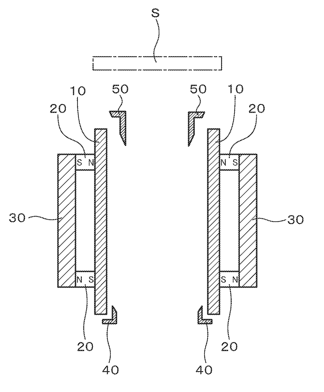
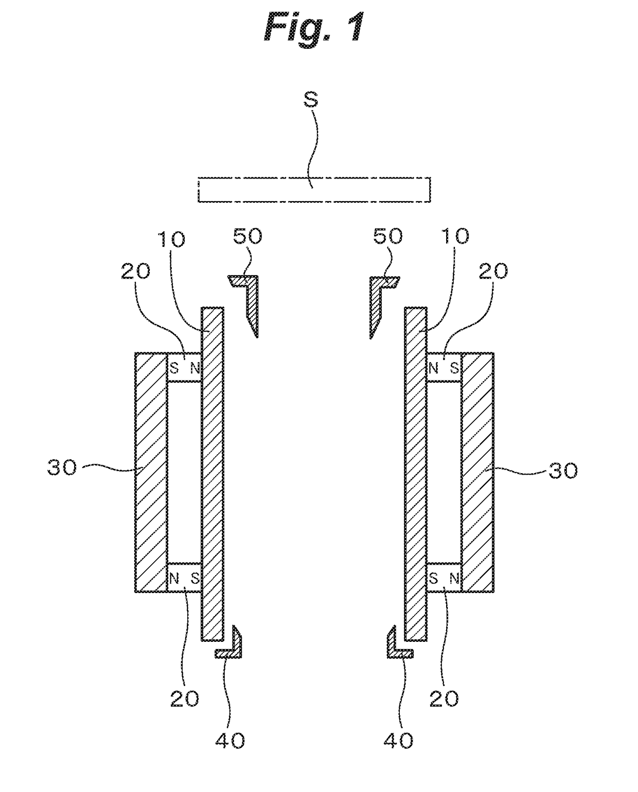
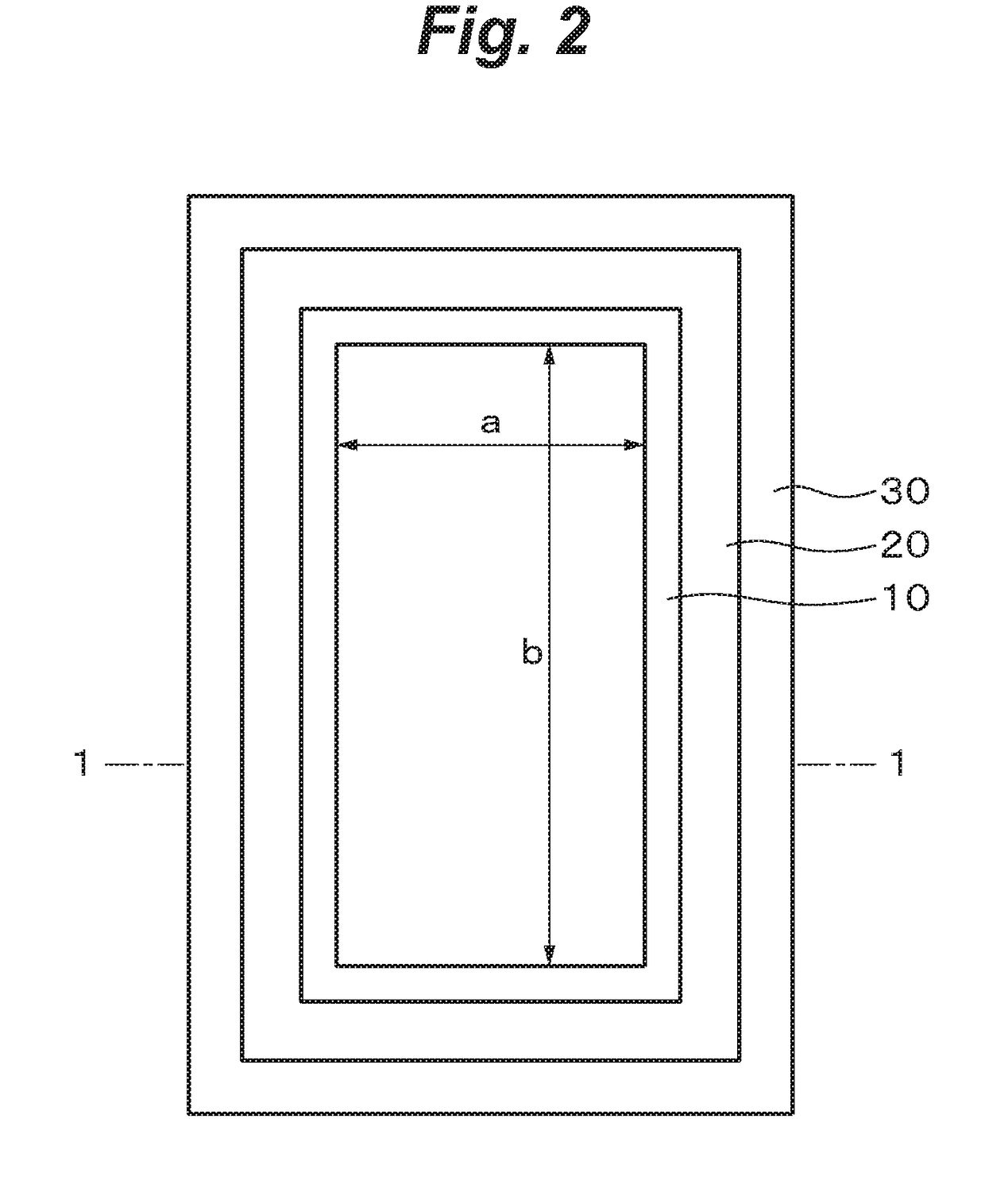
[0071]FIG. 1 and FIG. 2 are a longitudinal cross-sectional view and a plan view showing the sputtering device according to the first embodiment and show construction around a sputtering cathode and an anode disposed inside a vacuum chamber of the sputtering device. FIG. 1 is a cross-sectional view along the line 1-1 of FIG. 2.

[0072]As shown in FIG. 1 and FIG. 2, the sputtering device comprises a sputtering target 10 having a rectangular tubular shape in which the cross-sectional shape thereof is a rectangular, and an erosion surface faces inward, a permanent magnet 20 disposed outside the sputtering target 10 and a yoke 30 disposed outside the permanent magnet 20. The sputtering target 10, the permanent magnet 20 and the yoke 30 form the sputtering cathode. The sputtering cathode is generally fixed to the vacuum chamber in an electrically isolated state. The permanent magnet 20 and the yoke 30 form a magnet circuit. Although polarity of the per...

second embodiment

The Second Embodiment

[Sputtering Device]

[0082]In the sputtering device, the sputtering target 10 comprises the sputtering targets 10a, 10b, 10c and 10d shown in FIG. 9. Here, the sputtering targets 10a and 10b forming the long side sections facing each other are made of materials different from each other. Other construction of the sputtering device is as the same as the sputtering device according to the first embodiment.

[Method for Forming a Film by the Sputtering Device>

[0083]As the same as the first embodiment, film formation is performed in the film formation region of the substrate S by using the beams of sputtered particles 70 and 80. In this case, since the sputtering targets 10a and 10b are made of materials different from each other, constituent atoms of the beam of sputtered particles 70 and constituent atoms of the beam of sputtered particles 80 are different from each other. Therefore, the thin film F formed on the substrate S has the composition in which constituent at...

third embodiment

The Third Embodiment

[Sputtering Device]

[0085]FIG. 10 shows the sputtering device according to the third embodiment. In the sputtering device, as the same as the sputtering device according to the second embodiment, the sputtering target 10 comprises the sputtering targets 10a, 10b, 10c and 10d shown in FIG. 9, the sputtering targets 10a and 10c of the long side sections facing each other being made of materials different from each other. In addition, as shown in FIG. 10, in the sputtering device, a horizontal shield plate 90 held by a carrying mechanism not illustrated can be placed at a height between the height of the substrate S and the height of the light stopping shield 50 so as to stop the beam of sputtered particles 80 from the sputtering target 10c or the beam of sputtered particles 70 from the sputtering target 10a. Other construction of the sputtering device is as the same as the sputtering device according to the first embodiment.

[Method for Forming a Film by the Sputteri...


PUM

PropertyMeasurementUnit
Distanceaaaaaaaaaa
Distanceaaaaaaaaaa
Lengthaaaaaaaaaa

Abstract

This sputtering cathode has a sputtering target having a tubular shape in which the cross-sectional shape thereof has a pair of long side sections facing each other, and an erosion surface facing inward. Using the sputtering target, while moving a body to be film-formed, which has a film formation region having a narrower width than the long side sections of the sputtering target, parallel to one end face of the sputtering target and at a constant speed in a direction perpendicular to the long side sections above a space surrounded by the sputtering target, discharge is performed such that a plasma circulating along the inner surface of the sputtering target is generated, and the inner surface of the long side sections of the sputtering target is sputtered by ions in the plasma generated by a sputtering gas to perform film formation in the film formation region of the body to be film-formed.

Description

TECHNICAL FIELD[0001]This invention relates to a sputtering cathode, a sputtering device, and a method for producing a film-formed body, which are suitably applied to make various devices in which thin films are formed by a sputtering method.BACKGROUND ART[0002]Heretofore, in steps for forming electrodes in various devices such as semiconductor devices, solar batteries, liquid crystal displays, organic ELs, vacuum evaporation devices have been used to deposit electrode materials. However, a vacuum evaporation method has difficulties in controlling distribution of film thickness spatially and in time. Therefore, deposition of electrode materials by a sputtering method is desired.[0003]Heretofore, as sputtering devices, a parallel-plate, magnetron sputtering device, an RF sputtering device, a facing targets sputtering device, etc. have been known. Among them, in the facing targets sputtering device, two circular or square or rectangular targets made of the same materials having the sa...

Claims


Application Information

Patent Timeline
IPC IPC(8): C23C14/34H01J37/34
CPCC23C14/3407H01J37/342H01J37/3423H05H1/50C23C14/35C23C14/562H01J37/345H01J37/3452H01J37/3447H01J37/32752H01J37/3277F28F5/02F28F3/12H01J37/3405C23C14/352C23C14/564H01J37/3414H05H1/46C23C14/541H01J37/3411H01J37/3488
Inventor IWATA, HIROSHINEDU, TOSHIYUKITAKAKUWA, YUTAOKADA, NAOYASATO, IPPEISHIBATA, NAONORIHASHIMOTO, KEIICHI
Owner KEIHIN RAM TECH
Why Eureka
Try Eureka