Method for manufacturing an edge termination for a silicon carbide power semiconductor device

a technology of silicon carbide power semiconductor and edge termination, which is applied in the field of power electronics, can solve the problems of increasing alignment precision and reproducibility, reducing production yield, and high manufacturing cost, and achieves the effects of reducing the number of edge terminations

Active Publication Date: 2018-04-19
HITACHI ENERGY SWITZERLAND AG
View PDF2 Cites 10 Cited by
  • Summary
  • Abstract
  • Description
  • Claims
  • Application Information

AI Technical Summary

Benefits of technology

The invention provides a method for manufacturing an edge termination for a power silicon carbide semiconductor device that efficiently prevents or lowers any electric field peaks in the termination region, thereby improving the breakdown properties of the device. The method involves the use of a doping reduction layer, which can be implanted into the device using light ions such as helium or hydrogen (protons). This results in a device with higher blocking stability and lower leakage current. The doping reduction layer can be combined with existing termination means such as p doped guard rings, junction termination extensions, or floating metal rings. The use of a single or multiple ion peaks with different energies can further enhance the breakdown voltage without increasing the leakage current.

Problems solved by technology

This makes the manufacturing costly.
At the same time, it increases demands on the alignment precision and reproducibility of lithographical processing steps and / or it reduces production yield.
Due to the misalignment of highly and lightly doped p-regions in production, the enhancement of the blocking voltage might not be as high as predicted by the device simulation.

Method used


Image

  • Method for manufacturing an edge termination for a silicon carbide power semiconductor device
  • Method for manufacturing an edge termination for a silicon carbide power semiconductor device
  • Method for manufacturing an edge termination for a silicon carbide power semiconductor device

Examples


Embodiment Construction

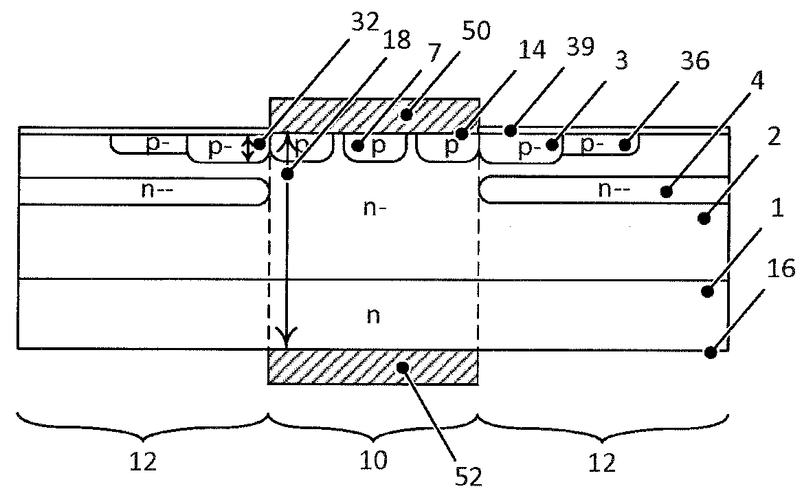
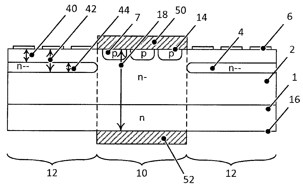
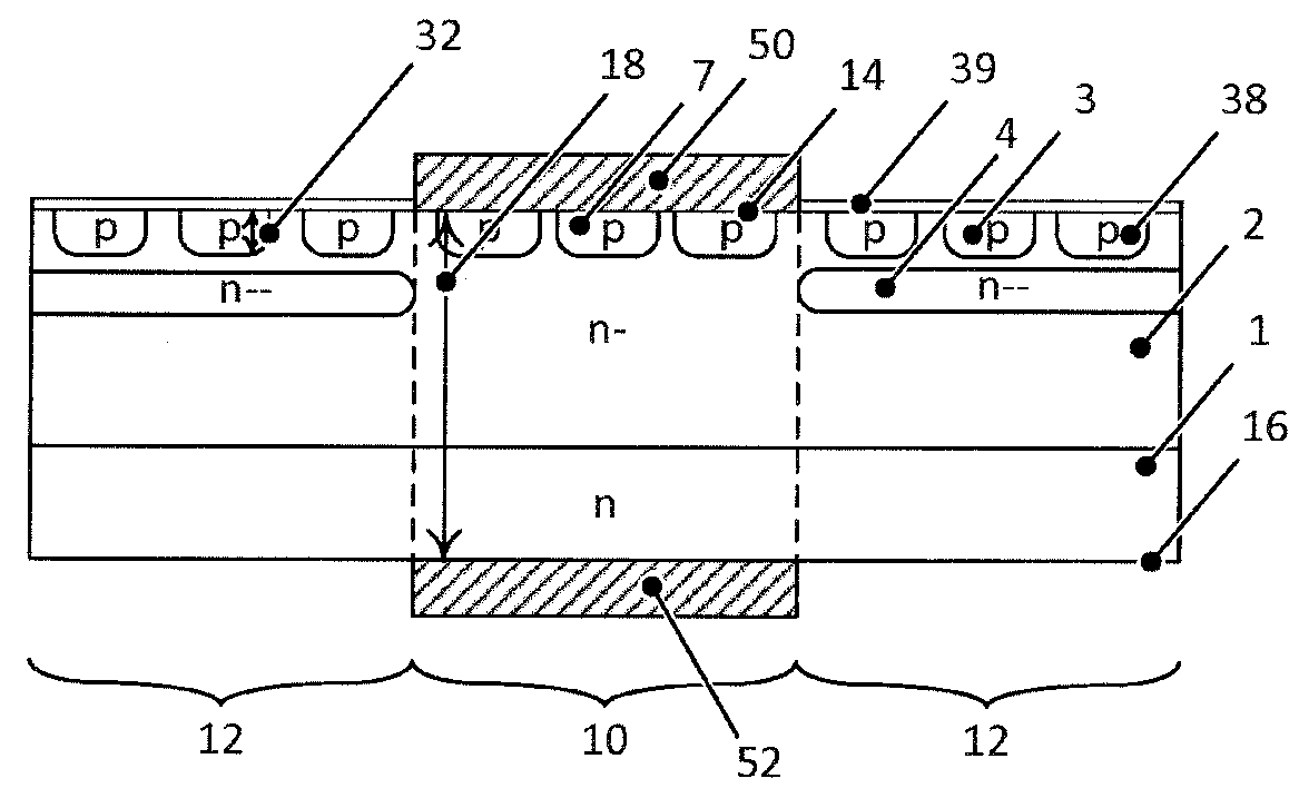
[0027]FIGS. 1 to 8 and 16 show an inventive silicon carbide power semiconductor device in form of a Junction Barrier Schottky (JBS) diode or a merged PiN Schottky (MPS) diode having a central region 10 and an edge region 12 (termination region) between a first main side 14 and a second main side 16 opposite to the first main side 14. An n doped silicon carbide substrate layer 1 is arranged on the second main side 16. An n− doped silicon carbide drift layer 2 which is lower doped than the n doped SiC substrate 1, is arranged on the first main side 14.

[0028]In the edge region 10 an (n−−) doped doping reduction layer 4 is arranged, which has a lower doping concentration than the drift layer 2, wherein the doping reduction layer 4 is arranged in a layer depth range 44 between a doping concentration minimum 40 below the first main side 14 up to a maximum doping reduction layer depth 42. This maximum depth 42 is lower than the thickness of the power semiconductor device. The doping concen...


PUM

PropertyMeasurementUnit
depthaaaaaaaaaa
depthaaaaaaaaaa
energyaaaaaaaaaa

Abstract

A method for manufacturing an edge termination structure for a silicon carbide power semiconductor device having a central region and an edge region is provided. The following manufacturing steps are performed: a) providing an n-doped silicon carbide substrate, b) epitaxially growing a silicon carbide n-doped drift layer on the substrate, which has a lower doping concentration than the substrate, c) creating at least one p-doped termination layer by implanting a second ion up to a maximum termination layer depth and annealing on the first main side, d) forming a doping reduction layer having a depth range, which doping reduction layer comprises at least one doping reduction region, wherein a depth of a doping concentration minimum of the doping reduction layer is greater than the maximum termination layer depth, wherein for the creation of each doping reduction region: implanting a first ion with an implantation energy in the drift layer at least in the edge region, wherein the first ion and the at least one implantation energy are chosen such that the doping reduction layer depth range is less than 10 μm, e) annealing the doping reduction layer, wherein step d) and e) are performed such that the doping concentration of the drift layer is reduced in the doping reduction layer.

Description

TECHNICAL FIELD[0001]The invention relates to the field of power electronics and more particularly to a method for manufacturing an edge termination structure for a silicon carbide power semiconductor device, to a method to manufacture a silicon carbide power semiconductor device having such an edge termination structure and to a silicon carbide power semiconductor device as such.BACKGROUND ART[0002]A conventional silicon carbide (SiC) Schottky diode comprises an n-type SiC substrate, on which an n− doped drift layer is epitaxially grown. This drift layer is contacted by a Schottky contact. Surrounding the Schottky contact a p doped junction termination extension (JTE) layer may be arranged in order to lower the electric field peak on the edge of the Schottky contact and to smoothly lower the electric field towards the edge of the diode. Additionally to the JTE layer, concentric floating p doped guard rings may be around the JTE layer to avoid high field peaks on the surface of the ...

Claims


Application Information

Patent Timeline
Patent Type & Authority Applications(United States)
IPC IPC(8): H01L29/872H01L29/16H01L29/06H01L29/66H01L29/739
CPCH01L29/872H01L29/1608H01L29/0619H01L29/6606H01L29/7395H01L29/868H01L29/0615H01L29/32H01L29/36H01L29/8083
Inventor VOBECKY, JAN
Owner HITACHI ENERGY SWITZERLAND AG
Why Eureka
Try Eureka