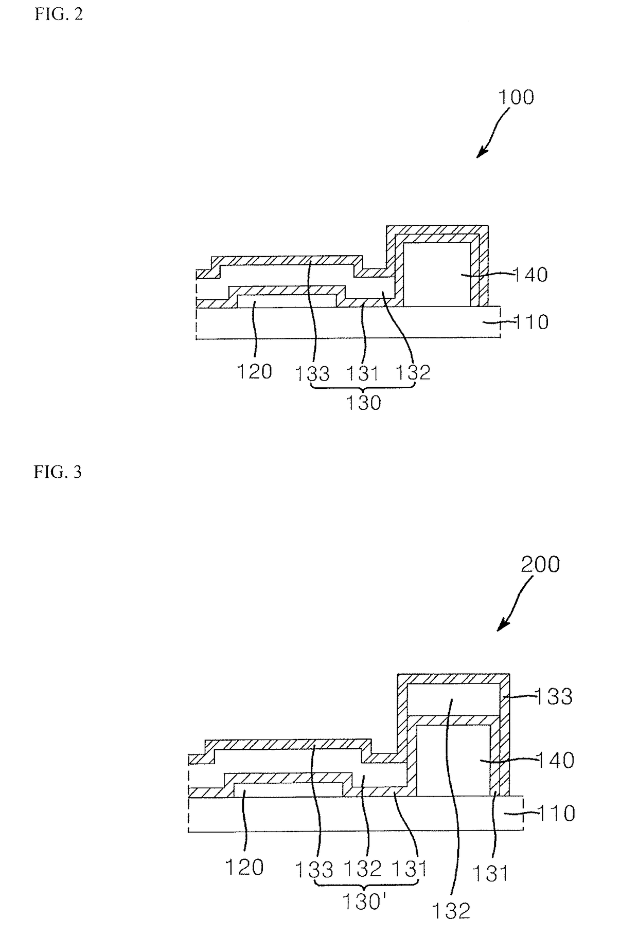
Organic light emitting display
a light-emitting display and organic technology, applied in the field of organic light-emitting displays, can solve the problems of organic light-emitting elements being vulnerable to moisture and/or oxygen, organic light-emitting elements being susceptible to delamination, etc., to achieve excellent transparency, low water vapor permeability, and high plasma resistance
- Summary
- Abstract
- Description
- Claims
- Application Information
AI Technical Summary
Benefits of technology
Problems solved by technology
Method used
Image


Examples
preparation example 1
[0159]In a 3,000 ml reactor equipped with a cooling tube and a stirrer, 300 ml of dichloromethane (Sigma Aldrich Corporation) was placed, and 200 g of 4-hydroxybutyl acrylate (Shin Nakamura Chemical Co., Ltd.) and 168 g of triethylamine were added, followed by cooling the temperature of the flask to 0° C., and adding dropwise a solution of 278 g of p-toluenesulfonyl chloride (Sigma-Aldrich Corporation) dissolved in 500 ml of dichloromethane, for 2 hours while stirring. After stirring for additional 5 hours, the remaining solvent was removed by distillation. The obtained compound 300 g was added to 1,000 ml of acetonitrile (Sigma Aldrich Corporation), and 220 g of potassium carbonate (Sigma Aldrich Corporation) and 141 g of 2-phenylphenol were added, followed by stirring at 80° C. Residual solvent and reaction residue were removed to obtain a compound of Formula 5 (molecular weight 296.36) having a purity of 93% as determined by HPLC.
preparation example 2
[0160]In a 2,000 ml flask equipped with a cooling tube and a stirrer, 600 ml of dichloromethane (Sigma Aldrich Corporation) was placed, and 58.8 g of 2-hydroxyethylmethacrylate (Sigma Aldrich Corporation) and 52.2 g of triethylamine (Sigma Aldrich Corporation) were added while stirring at 0° C., followed by slowly adding 100 g of triphenylchloromethane (Sigma Aldrich Corporation). After raising the temperature to 25° C., the mixture was stirred for 4 hours. After removing dichloromethane by distillation under reduced pressure, 124 g of a compound of Formula 6 having a purity of 97% as determined by HPLC was obtained using a silica gel column.
preparation example 3
[0161]In a 2,000 ml flask equipped with a cooling tube and a stirrer, 800 ml of acetonitrile (Fisher Scientific) was placed, and 180 g of potassium carbonate (Sigma Aldrich Corporation) and 108 g of acrylic acid were added while stirring at 0° C., followed by slowly adding 150 g of 4,4′-bis(chloromethyl)biphenyl (Tokyo Chemical Industry Co., Ltd.). After raising the temperature to 70° C., the mixture was stirred for 12 hours. After removing acetonitrile by distillation under reduced pressure, 177 g of a compound of Formula 7 having a purity of 97% as determined by HPLC was obtained using a silica gel column.
PUM
| Property | Measurement | Unit |
|---|---|---|
| thickness | aaaaa | aaaaa |
| thickness | aaaaa | aaaaa |
| thickness | aaaaa | aaaaa |
Abstract
Description
Claims
Application Information
 - R&D
- Intellectual Property
- Life Sciences
- Materials
- Tech Scout
- Unparalleled Data Quality
- Higher Quality Content
- 60% Fewer Hallucinations
Browse by: Latest US Patents, China's latest patents, Technical Efficacy Thesaurus, Application Domain, Technology Topic, Popular Technical Reports.
© 2025 PatSnap. All rights reserved.Legal|Privacy policy|Modern Slavery Act Transparency Statement|Sitemap|About US| Contact US: help@patsnap.com