Inrush current prevention circuit

a technology of inrush current and prevention circuit, which is applied in the direction of dc-dc conversion, power conversion system, electrical equipment, etc., can solve the problems of excessive inrush current flow, serious damage to capacitors or loads, and damage to power supplies,

Inactive Publication Date: 2017-09-21
FUJI ELECTRIC CO LTD
View PDF13 Cites 9 Cited by
  • Summary
  • Abstract
  • Description
  • Claims
  • Application Information

AI Technical Summary

Benefits of technology

[0037]According to embodiments of the disclosure, a bypass threshold (capacitor charging threshold) that forms a timing trigger for bypassing a high-resistance element such as a current limiting resistor is set in accordance with a voltage dividing ratio of a power supply voltage, because of which an excessive inrush current generated when the high-resistance element is bypassed can be prevented regardless of a rated input voltage range.

Problems solved by technology

When an excessive inrush current flows, there is concern that serious damage will be caused not only to the capacitor or a load, but also to the power supply.
However, the circuit of FIG. 4 is such that the charging threshold of the reference power supply 112 needs to be uniquely set in accordance with a lower limit of a rated input voltage range, meaning that when the rated input voltage range of the circuit is wide, there is a problem in that an inrush current when the FET 103 switches from an off-state to an on-state cannot be sufficiently restricted.
However, even when the rated input voltage range is, for example, 5 to 15V, the charging threshold has to be set in the region of 4.5V, meaning that when the input voltage is the maximum rated voltage of 15V, the drain-to-source voltage of the FET 103 when the FET 103 switches from an off-state to an on-state and the charging resistor 104 is bypassed is 10.5V, and there is a problem in that an excessive inrush current flows in via the FET 103.
According to the existing technology described in JP '448, an inrush current when starting up can be restricted, but because of the principle of causing one of the start-up circuit 140 or control circuit 163 to operate, a circuit utilization rate is low, which is wasteful in terms of circuit configuration and cost.

Method used


Image

  • Inrush current prevention circuit
  • Inrush current prevention circuit
  • Inrush current prevention circuit

Examples


first embodiment

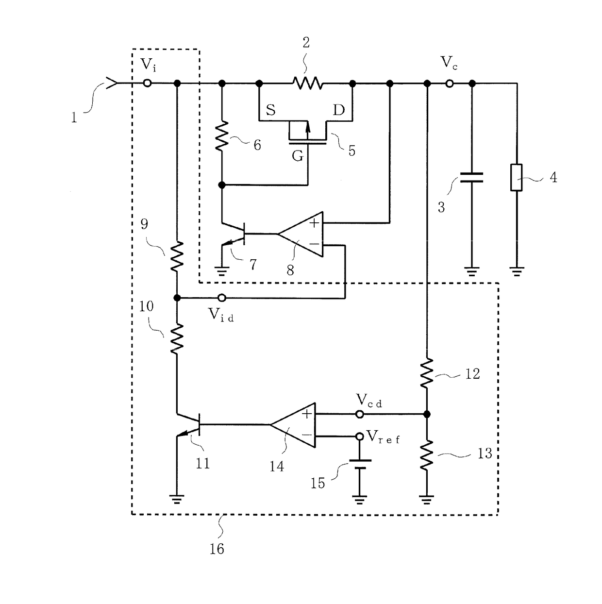
[0045]FIG. 1 shows an inrush current prevention circuit according to the disclosure. In FIG. 1, one end of each of capacitor 3 and load 4 is connected via a current limiting resistor 2 acting as a high-resistance element to a power supply input terminal 1, to which a direct current power supply (not shown) is connected.

[0046]The two ends of the current limiting resistor 2 are connected one each to a source S and drain D of a P-type MOSFET (hereafter referred to simply as an FET) 5 acting as a bypass element (a bypass switching element). Also, a pull-up resistor 6 and a second switching element 7 are connected in series between the power supply input terminal 1 and a ground point, and a connection point of the two is connected to a gate G of the FET 5.

[0047]The switching element 7 is a bipolar transistor, and an output signal of a second comparator 8 is applied to a base of the switching element 7. A voltage (output voltage) Vc of one end of the capacitor 3 is applied to a positive i...

second embodiment

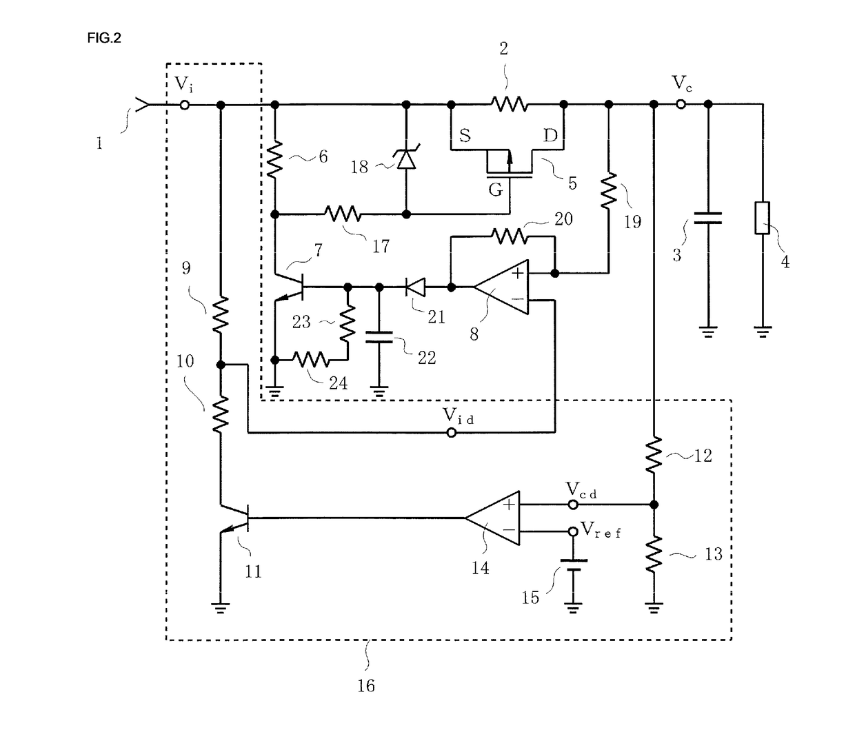
[0063]Next, based on FIG. 2, a description will be given of the disclosure.

[0064]In FIG. 2, the same reference sign is allotted to a portion having the same function as in FIG. 1, and a description thereof omitted, and the description hereafter centers on a portion differing from FIG. 1.

[0065]In FIG. 2, a resistor 19 is connected between the drain D of the FET 5 and the positive input terminal of the comparator 8, and a resistor 20 is connected between the positive input terminal of the comparator 8 and an output terminal. The resistors 19 and 20 are for applying hysteresis characteristics to the comparator 8 in accordance with a ratio of resistance values of the resistors 19 and 20.

[0066]Also, a diode 21, capacitor 22, and resistors 23 and 24, which configure a delay circuit, are connected between the output terminal of the comparator 8 and the switching element 7.

[0067]Furthermore, a Zener diode 18 is connected with the polarity shown in the drawing between the source S and gate G...

third embodiment

[0087]Next, FIG. 3 is a circuit diagram showing a main portion of the disclosure.

[0088]The third embodiment envisages a case wherein the rated input voltage range is extremely wide, multiple stages of the second comparator 8, second switching element 7, current limiting resistor 2, and FET 5 of the first and second embodiments are provided, and an inrush current at a time of a bypass operation is restricted by the FETs 5 being sequentially turned on in accordance with the magnitude of the voltage Vc of the capacitor 3.

[0089]In FIG. 3, n (n is a multiple) current limiting resistors 21 to 2n are connected in series between the power supply input terminal 1 and one end of the capacitor 3, and FETs 51 to 5n are connected in parallel to the resistors 21 to 2n respectively.

[0090]The drain D of the FET 51 on the capacitor 3 side is connected to each positive input terminal of n second comparators 81 to 8n provided corresponding to the current limiting resistors 21 to 2n, and each negative ...


PUM


Abstract

An inrush current prevention circuit, according to one possible configuration, includes: a power supply input terminal; a high-resistance element to restrict an inrush current flowing in when a power supply voltage is applied to the power supply input terminal; a low-resistance bypass element connected in parallel with the high-resistance element and configured to operate so as to cause current to bypass the high-resistance element when an output voltage being output from the inrush current prevention circuit to a load exceeds a bypass threshold; and bypass threshold setting circuit that divides the power supply voltage in accordance with the output voltage, and sets the bypass threshold in accordance with a voltage value of a voltage dividing point of the bypass threshold setting circuit.

Description

CROSS-REFERENCE TO RELATED APPLICATIONS[0001]This application is a continuation application, filed under 35 U.S.C. §111(a), of International Application PCT / JP2015 / 083689 filed on Dec. 1, 2015, the contents of which is incorporated herein by reference in its entirety.BACKGROUND[0002]1. Field[0003]The present disclosure relates to an inrush current prevention circuit that restricts an inrush current flowing when a power supply to an electronic circuit is turned on.[0004]2. Related Art[0005]When a power supply to an electronic circuit including a capacitor is turned on, a transiently extremely large current, that is, an inrush current, flows immediately afterward in order to charge the capacitor. When an excessive inrush current flows, there is concern that serious damage will be caused not only to the capacitor or a load, but also to the power supply.[0006]Therefore, there is widespread awareness of an inrush current prevention circuit wherein an inrush current is restricted by a hig...

Claims


Application Information

Patent Timeline
Patent Type & Authority Applications(United States)
IPC IPC(8): H02H9/02H02M1/32
CPCH02M1/32H02H9/025H02M3/156
Inventor HAMADA, YOSHITAKA
Owner FUJI ELECTRIC CO LTD
Why Eureka
Try Eureka